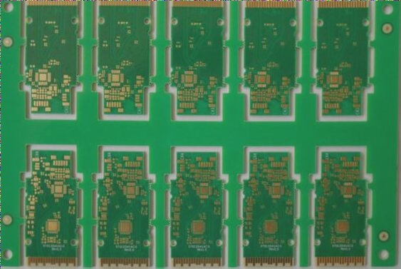
▪ In the mid-1990s, Japan and the European Union enacted relevant legislation. Japan mandated the elimination of lead solders in the electronics sector by 2001, while the EU set its deadline for 2004. The United States is also addressing this issue, aiming for complete adoption of lead-free products by 2008. Our country is actively researching and developing lead-free solutions to align with these global trends.
▪ When electronic products are discarded, the lead present in PCB solder can easily leach into oxygenated water, leading to water pollution and environmental harm. This solubility enables accumulation in the human body, resulting in nerve damage, fatigue, high blood pressure, anemia, reproductive issues, and other health problems; high levels may even lead to cancer. Valuing life, the current era demands lead-free PCB products.
2. Commonly Used Lead-Free Solder Ingredients

▪ Zinc can reduce the melting point of tin. However, if zinc exceeds 9%, the melting point will rise, and bismuth will decrease in the Sn-Zn mixture, while increasing bismuth also leads to greater brittleness.
▪ Zinc can lower the melting point of tin. If zinc increases beyond 9%, the melting point will rise, and bismuth content will decrease in the Sn-Zn alloy; yet, an increase in bismuth also results in increased brittleness.
▪ This composition is currently the most widely used lead-free solder. It demonstrates relatively stable performance, and its soldering parameters are similar to those of lead solder.
▪ Although indium can lower the liquidus and solidus temperatures of tin alloys, it presents issues such as thermal fatigue resistance, ductility, alloy embrittlement, and poor workability, making its use quite rare today.
Third, characteristics of lead-free solder
▪ The Sn-Ag-Cu alloy has a higher melting point (217 degrees Celsius) and can withstand high temperatures (260±3 degrees Celsius) effectively.
▪ Lead-free products are leaders in green environmental protection, promoting human health and are non-corrosive.
▪ Its specific gravity is slightly lower, comparable to that of tin.
▪ It exhibits poor liquidity.
Fourth, challenges in PCBA lead-free soldering
▪ The alloy’s structure renders it more brittle and less elastic compared to lead solder.
▪ The melting point of the liquidus and solidus for the Sn-Zn alloy will rise, but as bismuth content increases, the melting range widens; thus, bismuth reduces the melting point of the alloy and exacerbates brittleness compared to lead.
▪ Wettability is poor; the solder expands but does not contract. When copper is added to the Sn-Ag system, the eutectic point shifts. Eutectic formation occurs when silver increases by 4.8% and copper by about 1.8%. Adding indium enhances miniaturization strength and expansion characteristics, though it creates an oxide film that slightly impairs wettability.
▪ The color appears dull, and gloss is reduced.
▪ Phosphorus content limits the applicability of lead-free solder, affecting gloss but not other quality aspects.
▪ The defect rate for issues like tin bridging, voids, and pinholes needs to be minimized.
▪ Such defects are more prevalent than with lead solder, but they are not insurmountable. The type and quality of flux used are more critical than with lead, and the preheater temperature must be stable. The soldering times are: for the first wave, 1-1.5 seconds with a contact area of 10-13 mm; for the second wave, 2-2.5 seconds with a contact area of approximately 23-28 mm, while the board surface temperature should not exceed 140°C. Consequently, lead-free solder necessitates high-performance equipment, particularly regarding the spacing between double peaks. If too close, this may raise board temperatures, increase component damage, promote flux volatilization, and lead to excessive defects such as tin bridges.


