Challenges and Solutions in Miniaturized PCB Production
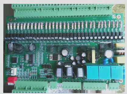
In recent years, the PCB manufacturing industry has faced increasing demands for miniaturization and thinning of electronic components, driven by the performance requirements of smart terminal devices like smartphones, tablets, and wearable tech.
One critical aspect of PCB production is the solder paste printing process, which accounts for over 60% of defects in the Surface Mount Technology (SMT) industry. Addressing issues in solder paste printing is key to overcoming challenges in the entire SMT workflow.
Key Points:
- British 01005 SMD devices and 0.4 pitch BGA/CSP are widely used in SMT production.
- Metric 0201 SMD devices are in trial production, with expectations for increased adoption.
- Understanding the area ratio of stencil printing is crucial for addressing challenges posed by miniaturized components.
Solutions for Solder Paste Printing:
When dealing with miniaturized pads, the thickness of the steel mesh and the area ratio of openings play a significant role in successful solder paste printing.
1. Reduce Steel Mesh Thickness:
By using a thinner steel mesh with increased opening area ratio, soldering on small component pads can be improved. However, for substrates with large components, alternative solutions may be needed to prevent insufficient soldering.
2. Utilize Advanced Steel Mesh Technologies:
There are several innovative steel mesh options available:
- FG (Fine Grain) steel mesh: Incorporates niobium for cleaner and smoother hole walls, improving demolding.
- Electroformed steel mesh: Features smooth hole walls and customizable thickness, but comes at a higher cost.
- Ladder steel mesh: Offers selective thickening or thinning for different pad requirements.
- Nano coating (Nano Ultra Coating): An advanced coating technology for enhanced solder paste release.
These solutions aim to optimize solder paste printing for miniaturized components, ensuring efficient production processes in the evolving PCB manufacturing landscape.
Enhancing Solder Paste Printing Quality with Nano-Coating
Applying nano-coating on the steel mesh surface can improve demolding effectiveness and ensure consistent solder paste volume stability during printing. This leads to higher print quality and reduces the need for frequent cleanings of the steel mesh. While many domestic processes only use a single layer of nano-coating, some international practices involve directly plating the steel mesh with nano-coatings for enhanced performance and durability, albeit at a higher cost.
Dual Solder Paste Molding Processes
-
Printing/Printing
This method involves using two printing machines: one with a standard stencil for fine-pitch small component pads, and the second with a 3D stencil or stepped stencil for large component pads. While effective, this approach requires two printers and increases stencil costs, especially when a 3D stencil and comb-shaped scraper are used, impacting production efficiency.
-
Printing/Spray Tin
In this scenario, the first solder paste printer manages small component pads, while a second inkjet printer applies solder paste to large component pads. Although this method results in good solder paste formation, it can be costly and less efficient, particularly depending on the quantity of large component pads.
Users can choose between these solutions based on their specific needs. To balance cost and production efficiency, options such as reducing stencil thickness, using stencils with lower aperture area ratios, and adopting stepped stencils are generally more suitable. For users with low output but high quality requirements, and who are less cost-sensitive, the printing/jet printing option may be more suitable.