Common Issues with PCB Warpage in Electronic Manufacturing
- PCB warpage can cause shifts in SMT component feeding positions, impacting product quality.
- Warped PCBs may lead to incomplete soldering and compromise product durability.
- Insufficient board strength can result in depressions in large-area PCBs.
- Uneven PCB foundations can lead to incomplete soldering and assembly issues.
- Minor warpage can affect circuit function stability, while severe cases may cause malfunctions.
- Flatness of PCBs significantly influences production yield in automated environments.
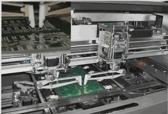
In modern electronic manufacturing, automated SMT processes are crucial for high-speed production. Automatic feeding and soldering operations are managed by machinery to ensure efficiency and accuracy. However, PCB warpage poses challenges in maintaining product quality and stability.
Impact of PCB Warpage on Automated Production
- Warped PCBs can lead to decreased product quality and stability, resulting in higher costs due to reprocessing.
- Uneven PCBs during SMT processing may cause malfunctions in insertion machines, slowing down production.
- Skewed components from PCB warpage can complicate chassis assembly and increase labor costs.
- Accurate feeding is crucial in SMT automation to ensure proper component placement and soldering.
- Issues like component ejection and misalignment can arise from PCB warpage, affecting soldering quality.
- Uneven PCBs can cause material ejection, positional shifts, and soldering errors in semiconductor components.
Addressing PCB warpage is essential for optimizing automated production processes and maintaining high-quality electronic products.
Minimizing PCB Deformation in Manufacturing
- IPC standards recommend keeping PCB deformation below 0.75% for automated SMT processing.
- Manual loading/soldering allows up to 1.5% deformation, but precision demands stricter control.
- Understanding PCB warping origins is crucial due to material variations and processing complexities.
- Factors like copper area variations and circuit layout significantly impact PCB flatness.
- HDI PCBs face challenges with connection points and thermal expansion, leading to warping.
- Optimizing design, material selection, and production processes can help minimize PCB deformation.
- Considerations like copper layer thickness, material characteristics, and handling practices are vital in preventing warpage.
- Processing-related deformation, stemming from mechanical and thermal stress, is a common issue in PCB manufacturing.
Addressing PCB Warpage Challenges
In the realm of PCB manufacturing, controlling deformation is essential for ensuring product quality and performance. By delving into the intricacies of materials, design elements, and production processes, manufacturers can mitigate warping issues and enhance the reliability of their PCBs.
Key Strategies for Minimizing PCB Deformation
Effective solutions to PCB warping involve a holistic approach that encompasses material selection, design optimization, and meticulous attention to manufacturing processes. By proactively addressing factors that contribute to deformation, manufacturers can achieve greater precision and consistency in their PCB production.