Basically, the purpose of setting test points is to ensure that the components on a PCB meet the specifications and solderability standards. For instance, to verify the integrity of a resistance component on the PCB, the simplest method involves using a multimeter to measure across both ends.
However, in mass production facilities, it’s impractical to individually test every resistor, capacitor, inductor, and integrated circuit (IC) on each board using an electric meter. Hence, the introduction of ICT (In-Circuit-Test) automated testing machines, equipped with multiple probes commonly known as “Bed-Of-Nails” fixtures. These fixtures make simultaneous contact with all the parts on the board requiring measurement. Subsequently, the electronic components are sequentially measured through programmed control, with parallel testing used as a supplementary method. Typically, testing a general board’s components takes around 1 to 2 minutes, the duration dependent on the circuit board’s complexity—more components result in longer testing times.
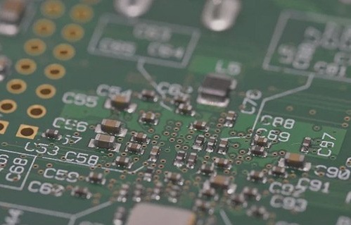
Direct contact between probes and electronic components or their solder joints risks damaging the components. To mitigate this, ingenious engineers devised test points, leading out additional connections at both ends of the components. These test points typically consist of small round dots without a solder mask, allowing test probes to make contact without directly affecting the measured electronic components.
In the past, when PCBs predominantly featured through-hole components (DIP), the solder joints of these components served as test points due to their robustness against probe pressure. However, with the advent of surface mount technology (SMT), the residues from solder paste flux post-wave soldering often caused poor probe contact due to their high resistance. This led to test operators resorting to methods such as using air spray guns or alcohol wipes to improve contact.
Even after wave soldering, test points may suffer from poor probe contact. However, with the widespread adoption of SMT, the reliability of testing significantly improved, thanks to the use of test points. SMT components are delicate and cannot withstand the direct pressure exerted by test probes. By using test points, direct contact between probes and components or their solder joints is avoided, thereby safeguarding components from damage. Consequently, this indirect approach greatly enhances test reliability by reducing instances of misjudgment.