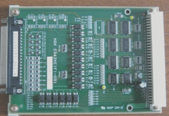
Matters to Keep in Mind During PCB Manufacturing Process
-
Regarding PADS Design
1. When working with double-sided PADS files, ensure that the hole attribute is set to through-hole to prevent missing drilling.
2. Avoid adding slot holes in PADS design with components as it may cause issues with GERBER generation. Add slots in DrillDrawing instead.
3. Copper in PADS should be paved using the Hatch method. After moving the original file, re-coating is necessary to prevent short circuits.
-
PROTEL99SE and DXP Design Documents
1. Solder mask in PROTEL99SE is based on the Solder mask layer. Move to the solder mask layer if GERBER generation for solder paste layer is needed.
2. Avoid locking the outline in Protel99SE to ensure proper GERBER generation.
3. Do not select the KEEPOUT option in DXP files to prevent issues with GERBER generation.
4. Pay attention to the design of the front and back layers in PROTEL99SE and DXP. Top layer should be orthographic, bottom layer should be reversed.
-
Other Important Considerations
1. Place shapes like plate frames and slots on the KEEPOUT or mechanical layer, not on silk screen or circuit layers.
2. Ensure consistency between mechanical and KEEPOUT layer shapes. Provide effective shapes and special instructions if needed.
3. Pay attention to exposing button bits to copper in three software designs.
4. When making metallized slots, group multiple pads together.
5. Note if chamfering is required for gold finger boards.
6. Check GERBER files for correct layering before ordering.
7. Follow standard naming conventions for GERBER files.