Optimizing Inductor Placement for Efficient PCB Design
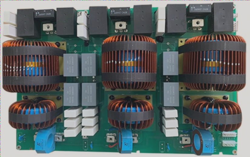
Switching regulators, crucial for voltage conversion, utilize inductors to store energy temporarily. These inductors, integral components in a printed circuit board (PCB), require strategic integration. Attention to detail is key, as the current flow through the inductor fluctuates gradually but continuously.
Switching regulators alternate current flow between two paths at high speeds, determined by the switching edges’ characteristics. The path through which the current flows, known as the *thermal loop* or *AC current path*, conducts current in one state and not in the other.
When designing a PCB layout, minimizing the thermal loop’s area and keeping its path short are critical. This minimizes parasitic inductance, reducing voltage fluctuations and electromagnetic interference (EMI), thus enhancing the regulator’s efficiency.
Enhancing Control Trace Routing Near Inductors
When designing PCBs for switching regulators, special attention must be paid to routing sensitive control traces, particularly around inductors. Avoid routing sensitive paths beneath an inductor, whether on the surface, inner layers, or back of the PCB, to prevent magnetic field interference.
Inductors exhibit capacitive behavior, affecting nearby traces. To minimize interference, keep sensitive traces away from inductors. Some designers even eliminate copper under the inductor to prevent eddy currents, although maintaining an uninterrupted ground plane offers benefits like shielding efficiency and improved heat dissipation.
- Shielding Efficiency: An unbroken ground plane shields signals from external noise.
- Improved Heat Dissipation: Continuous copper enhances thermal management.
- Eddy Current Considerations: While eddy currents under the inductor are localized, they have minimal impact on the ground plane’s performance.
It is generally recommended to keep the ground plane intact under the inductor unless there are significant thermal or interference issues. By prioritizing signal integrity and heat dissipation, efficient PCB design can be achieved.