PCB Board Design Inspection Checklist
- Analysis and Division of Circuit into Basic Units
- Utilization of Short or Isolated Key Leads
- Identification and Implementation of Shielding
- Utilization of Basic Grid Graphics
- Appropriateness of Printed Board Size
- Optimal Wire Widths and Spacing
- Usage of Preferred Pad and Hole Sizes
- Suitability of Photographic Plates and Sketches
- Minimization of Jumper Wires
- Legibility and Correctness of Labels
- Prevention of Copper Foil Blistering
- Presence of Tool Positioning Holes
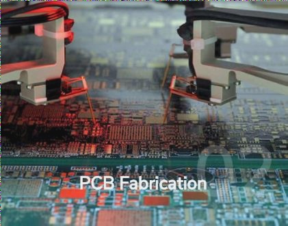
PCB Board Electrical Characteristics Inspection
- Analysis of Wire Resistance, Inductance, and Capacitance
- Insulation Requirements for Wire Accessories
- Control of Insulation Resistance Value
- Polarity Identification
- Leakage Resistance and Voltage Influence
- Impact of Surface Coating Alteration
PCB Board Physical Characteristics Inspection
- Suitability of Pads and Positions
- Shock and Vibration Resistance
- Spacing of Standard Components
- Proper Installation of Components
- Heat Dissipation and Cooling
- Positioning of Components
- Arrangement for Easy Inspection
- Elimination of Interference
- Verification of Positioning Holes
- Tolerance and Coating Properties
- Hole Diameter to Lead Wire Ratio
PCB Board Mechanical Design Factors
- Support Points Placement
- Size and Shape Considerations
- Mechanical Accessories
- Environmental Adaptability
- Mounting Orientation
- Support Requirements
- Secure Mounting
- Ease of Removal
Installation Requirements for Printed Circuit Boards
- Support Guidelines
- Spacing of Support Points
- Mounting Technology Factors
- Equipment Space Consideration
- Heat Dissipation Needs
- Shieldability Requirements
- Relationship with Other Circuits
Dial-Out Requirements for Printed Boards
- No Mounting Components on Printed Board Area
- Installation Distance Considerations
- Design of Mounting Holes and Slots
- Size Consideration of Plug-In Tools
- Securing Plug-In Devices with Rivets
- Inclusion of Load Bearing Flanges
- Adapting Tools to Board Specifications
- Cost and Accessibility Considerations
PCB Board Design: Key Mechanical Factors to Consider
When designing a PCB board, it is crucial to take into account various mechanical considerations that can significantly impact the overall performance and reliability of the printed board structures.
Substrate Properties
- Water absorption
- Coefficient of thermal expansion
- Flexural strength
- Impact strength
The substrate properties, such as water absorption and coefficient of thermal expansion, play a vital role in determining the functionality and productivity of the PCB board. Different dielectric backing materials, such as phenolic impregnated paper and epoxy impregnated glass cloth, also need to be carefully considered.
PCB Wire Spacing
Proper spacing of conductors is essential to prevent voltage breakdown or arcing. Factors like peak voltage, atmospheric pressure, and capacitive coupling parameters must be taken into account when determining the spacing between wires. Components with critical impedance or high frequency should be placed close together to reduce delays, while transformers and inductive components should be isolated to avoid coupling and noise issues.
PCB Board Wire Pattern Inspection
- Ensure wires are short and straight without compromising functionality
- Adhere to limitations on wire width
- Maintain proper distances between wires, mounting holes, and pads
- Avoid parallel arrangement of wires and close proximity with component leads
- Avoid acute angles in wire patterns on the PCB board
Latest Trends in PCB Design
Recent advancements in PCB technology have led to the development of flexible PCBs, which offer increased design flexibility and space-saving benefits. Additionally, the integration of Internet of Things (IoT) capabilities into PCBs is becoming more prevalent, enabling enhanced connectivity and functionality in various electronic devices.

