PCB Board Design Process
1. Netlist Input
At the beginning of the PCB board design process, the netlist provided by the circuit designer is imported. This netlist contains crucial information about the electrical connections between components on the PCB.
2. Rule Setting
Once the netlist is imported, the next step involves setting up design rules for the PCB layout. These rules define trace widths, clearances, and other parameters to ensure the design meets the necessary electrical and manufacturing requirements.
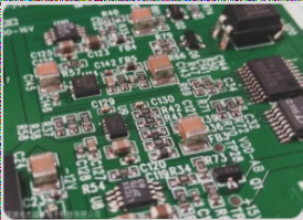
3. Component Layout
With the design rules in place, the designer can start placing components on the PCB board. Factors such as component placement, signal integrity, and thermal management must be carefully considered during this step.
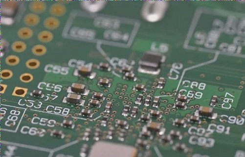
4. Wiring
After placing the components, the designer can begin routing the traces to connect the components based on the netlist. It is crucial to avoid signal interference and ensure the proper functioning of the PCB.
5. Inspection and Review
Once the wiring is complete, a thorough inspection of the layout is necessary to identify any errors or issues. Reviewing the design ensures that the PCB meets all requirements and functions correctly.
6. Output
The final step in the PCB design process is to generate the required output files for manufacturing. These files include Gerber files, bill of materials (BOM), and assembly drawings essential for producing the PCB board.
Latest Updates:
- PowerPCB board offers both manual and automatic component layout methods for efficient PCB design.
- Decoupling capacitors should be placed as close as possible to the VCC of the device for optimal performance.
- Effective communication and collaboration among team members are crucial for a successful PCB design project.

PCB Layout Best Practices
Consider Future Soldering and Efficient Layout
- When placing devices, consider future soldering and avoid dense layouts.
- Utilize Array and Union functions in your software for improved layout efficiency.
Wiring Techniques
There are two main wiring methods: manual wiring and automatic routing.
Manual Wiring
- Manually lay out important networks before automatic wiring, such as high-frequency clocks and main power supplies.
- Adjust PCB wiring after automatic routing to ensure optimal layout.
Auto-Routing
After manual routing, utilize the autorouter for the remaining network.
- Start the Specctra router interface, set the DO file, and initiate automatic wiring.
- Adjust routing manually if needed after the automatic process.
Key Notes
- Ensure power and ground wires are thick.
- Directly connect decoupling capacitors to VCC when possible.
- Protect manually routed wires from autorouting by adding the “Protect all wires” command.
- Define mixed power supply layers as Split/Mixed Plane and use Plane Connect for copper cladding.
- Set all device pins to thermal pad mode for optimal performance.
- Enable DRC and use Dynamic Route during manual routing.
Inspection and Review
Check for Clearance, Connectivity, HighSpeed, and Plane using the VerifyDesign tool. Review design rules, layer definitions, and routing rationality.
Design Output
Output PCB designs to a printer or as light drawing files for manufacturing.
- Output necessary layers including wiring, power, silk screen, and solder mask layers.
- Ensure proper settings for Split/Mixed power layers and Plane Connect before outputting light drawing files.
- Set up layers correctly for each component and silk screen layer.
Important Tips for PCB Design
- When working on the solder mask layer, remember to set the Layer properly. Select the via hole if you don’t want any solder mask on it, and avoid selecting the via hole if you want the solder mask to cover it. Always consider the specific requirements of the project.
- When creating the drilling file, stick to the default settings of the PowerPCB board. Avoid making unnecessary changes that could lead to errors in the manufacturing process.
- Once all the necessary files are generated, ensure to open and print them using CAM350. It is crucial to have the designs checked thoroughly by both designers and reviewers following the guidelines outlined in the “PCB Board Checklist” to guarantee accuracy and quality.