
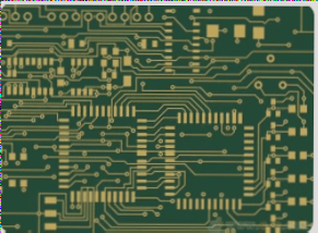
Optimizing PCB Layout for Efficient Power Supply Design
A well-designed PCB plays a crucial role in optimizing efficiency, reducing thermal stress, and minimizing noise and interference between traces and components in a power supply system.
Understanding Current Conduction Paths and Signal Flow
Designing a PCB layout starts with a deep understanding of current conduction paths and signal flow within the power supply, ensuring proper functionality and minimal heat generation.
Addressing Common Issues in Switching Power Supplies
One common issue in switching power supplies is unstable switching waveforms, which can lead to audible noise from magnetic components. Pinpointing and resolving layout-related issues can be challenging.
Collaboration for Effective Layout Design
Collaboration between power supply designers and PCB layout designers is essential to address critical layout considerations early in the design process, enhancing power efficiency and reducing noise.
Key Considerations for Power Supply Layout
- Place power supply output close to load device for voltage regulation
- Minimize interconnect impedance and conduction voltage drop
- Ensure proper airflow to reduce thermal stress
- Avoid obstructing airflow around passive components
- Shield sensitive signal traces from switching noise
Strategies for Multi-Layer Boards
On multi-layer boards, inserting a DC ground or voltage layer between high-current power components and small-signal traces can provide effective shielding. Ground and voltage planes should ideally not be separated to minimize noise impact.
Effective Power Stage Layout
The Importance of Power Supply Circuit Design in PCB Layout
- Power Stage and Control Circuit Division
- High DV/DT Switch Area
- Power Pad Form
- Control Circuit Layout
The power stage and small-signal control circuit are two main sections of a switching power supply circuit. To reduce PCB inductance, resistance, and voltage drop, high-current traces should be short and wide. Using high-frequency decoupling capacitors with low ESL and ESR values is crucial for handling high di/dt pulse currents.
To minimize EMI, keep the switch junction area small. Grounded copper areas can shield the switch junction and aid in heat dissipation. Balancing noise reduction and heat dissipation is key for high dv/dt switch junction design.
Proper placement of positive and negative vias for decoupling capacitors reduces ESL. Well-designed pad forms limit noise, thermal resistance, and impedance. Avoid overuse of thermal relief pads to prevent increased impedance and power losses.
Isolate control circuits from noisy areas and position them strategically based on the converter type. Maintain distance between control ICs and power components to reduce noise and heat. Separate signal ground and power ground, and connect them at a single point to ensure clean grounding.
Reducing Noise Coupling in PCB Design
- Capacitive coupling can occur between adjacent conductors, leading to noise interference.
- Avoid routing noisy switch traces near small-signal traces to minimize interference.
- Route high-noise traces on separate layers using the internal ground plane as a shield.
- Maintain a small distance between control IC and power components to reduce noise and heat impact.
- Use short, wide traces for gate drive signals to minimize impedance.
- Properly route FET driver traces with appropriate loop area to reduce inductance and noise.
- Current sense traces are sensitive and should be routed in parallel for noise reduction.
Trace Width Selection:
- Choose trace width based on current levels and noise susceptibility.
- Small-signal traces use narrower widths (10-15 mils), while high-current networks require wider traces (20 mils minimum).
If you have any PCB questions, feel free to reach out to us at info@wellcircuits.com.
 العربية
 简体中文
简体中文 Nederlands
 English
 Français
 Deutsch
 Italiano
 日本語
日本語 한국어
한국어 Português
 Русский
 Español
 ไทย
ไทย