This document aims to elucidate the printed circuit board design process and essential precautions when using PADS’s PowerPCB software. It also provides design specifications for designers within a working group, enhancing communication and mutual inspections among team members.
2 Design process
The PCB design process encompasses six key steps: netlist input, rule setting, component layout, wiring, inspection, review, and output.
2.1 Netlist input
There are two methods for entering the netlist. The first utilizes PowerLogic’s OLE PowerPCB CONnection function; by selecting Send Netlist, designers can ensure the schematic and PCB diagrams remain synchronized, reducing error potential. Alternatively, the netlist can be directly loaded in PowerPCB by navigating to File->Import and inputting the netlist generated from the schematic diagram.
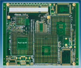
2.2 Rule Settings
If the PCB design rules have been established during the schematic design stage, there’s no need to set them again, as the design rules will be imported into PowerPCB along with the netlist. If any design rules are modified, the schematic must be synchronized to ensure consistency with the PCB. Besides design rules and layer definitions, there are additional rules to set, such as PadStacks, which necessitate adjustments to the size of standard vias. If a designer creates a new pad or via, Layer 25 must be included.
Note: PCB design rules, layer definitions, via settings, and CAM output settings are included in the default startup file named Default.stp. After entering the netlist, assign power and ground networks to the appropriate power layers and set other advanced rules based on the design’s actual requirements. Once all rules are established, use the Rules From PCB function of OLE PowerPCB Connection in PowerLogic to update the schematic rule settings, ensuring consistency between the schematic and PCB.
2.3 Component Layout
Once the netlist is entered, all components will initially be placed at the origin of the workspace and will overlap. The next step is to separate these components and arrange them neatly according to established rules, which is referred to as component layout. PowerPCB offers two methods: manual layout and automatic layout.
2.3.1 Manual Layout
1. Draw the board outline (Board Outline) to define the structure size of the printed circuit board.
2. Disperse the components (Disperse Components) so that they are arranged around the board’s edges.
3. Move and rotate each component individually, placing them within the board’s edge and arranging them neatly according to specific guidelines.
2.3.2 Auto Layout
PowerPCB provides both automatic layout and automatic local cluster layout; however, for most designs, the results may not be satisfactory, and this method is not recommended.
2.3.3 Matters Needing Attention
a. The primary principle of layout is to ensure wiring efficiency. Be mindful of the connections when relocating devices and group connected devices together.
b. Keep digital devices separate from analog devices and as far apart as possible.
c. Position decoupling capacitors as close as possible to the VCC of the device.
d. When placing components, consider future soldering; avoid placing them too densely.
e. Utilize the Array and Union functions provided by the software to enhance layout efficiency.
2.4 Wiring
Wiring can be performed using either manual wiring or automatic wiring. PowerPCB’s manual wiring functionality is robust, including features for automatic pushing and online design rule checking (DRC). Automatic wiring is handled by the Specctra wiring engine. Typically, these two methods are used in conjunction, following a common sequence of manual-automatic-manual.
2.4.1 Manual Wiring
1. Before initiating automatic wiring, manually lay out critical networks such as high-frequency clocks and main power supplies, which often have specific requirements for distance, line width, spacing, and shielding. Additionally, for specialized packages like BGA, regular automatic wiring can be challenging, necessitating manual routing.
2. After automatic routing, further adjustments to the PCB routing may be required through manual adjustments.
2.4.2 Automatic Wiring
Once manual wiring is completed, the remaining networks can be handed over to the automatic router. Select Tools->SPECCTRA to launch the Specctra router interface, set the DO file, and press Continue to initiate the automatic wiring process. If the wiring completion rate reaches 100%, manual adjustments can then be made; if it does not, this indicates potential issues with the layout or manual wiring that need to be resolved before all connections are established.
2.4.3 Matters Needing Attention
a. Use thicker traces for power and ground wires.
b. Connect decoupling capacitors directly to VCC whenever possible.
c. When setting the Specctra DO file, include the Protect All Wires command to safeguard manually routed wires from being altered by the automatic router.
d. If there is a mixed power layer, define it as Split/Mixed Plane, ensuring division before wiring. After wiring, utilize PourManager’s Plane Connect for copper pour.
e. Set all device pins to thermal pad mode by filtering to Pins, selecting all pins, modifying properties, and checking the Thermal option.
f. Enable DRC during manual routing and utilize dynamic routing (Dynamic Route).
2.5 Inspection
Items to be checked include Clearance, Connectivity, HighSpeed, and Plane. These can be selected via Tools->Verify Design. If high-speed rules are set, they must be verified; otherwise, this step can be skipped. If any errors are detected, modifications to the PCB layout and wiring will be necessary.
—
If you have any further requests or adjustments, feel free to ask!

