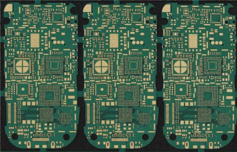
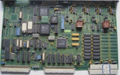
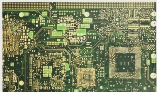
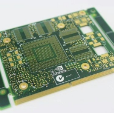
Noise Countermeasures on Printed Circuit Boards
The design process of a PCB often faces challenges, especially concerning the substrate, layout, and routing. Addressing these challenges is crucial for effective noise control on printed circuit boards.
Categorizing Circuits on a PCB
- Power/Ground circuit
- Main signal circuit
- Interface circuit
The interface circuit is vital for connecting the PCB to external signals. It plays a key role in noise control by preventing external noise from entering the PCB and ensuring internal noise does not radiate out. The power/ground circuit provides power to the signal and interface circuits, with the ground plane acting as the return path for unbalanced circuits.
Key Strategies for Noise Mitigation
- Stabilizing Potential: Maintaining stable potential for both power supply and ground is essential, despite the common impedance they share.
- Organized Layout: PCB substrate layout should align with the type and purpose of each circuit for effective noise mitigation.
- Separating Circuits: Ideally, high-noise-sensitive circuits should be separated from low-noise immunity circuits to minimize noise risks.
- Component Layout: Component arrangement is crucial for implementing effective routing principles.
- Interface Circuits: Digital circuits communicate through interface circuits, interacting with external systems.
- Analog Circuits: Analog circuits interface with external analog signals, requiring careful placement of components to prevent noise interference.
- Ground Design: Both digital and analog circuits should connect to a single ground point with an irregular pattern to separate units.
- Bypass Capacitors: Placing bypass capacitors at the power entry point stabilizes voltage and reduces noise.
- LC Filters: Inductors and bypass capacitors can be combined to form LC filters, crucial for noise control.
- Bypass Capacitor Placement: Bypass capacitors should be strategically placed based on current demand and frequency requirements.
PCB Design Best Practices for Noise Control
- A crucial aspect of PCB design is the placement of bypass capacitors near each IC to minimize inductance and improve effectiveness.
- Utilizing the “Beta pattern” for power and ground planes on multilayer PCBs offers lower impedance and better noise control, enhancing overall performance.
- Signal line design principles emphasize minimizing length and considering return paths to avoid large area loops that can introduce interference.
- To prevent crosstalk, separate low-noise signal lines from high-noise ones and carefully manage shared ground traces between signals.
- High-impedance circuits require shorter traces for improved noise immunity, while low-impedance circuits can accommodate longer traces with proper buffering.
- With increasing signal frequencies, addressing connection issues becomes more critical, necessitating solutions beyond traditional filtering methods.
- Terminating signals at the receiving end can help eliminate connections and reduce noise, enhancing energy efficiency and signal integrity.
PCB manufacturers are continuously developing practical techniques for effective EMI noise mitigation in modern PCB designs.