PCB Design Best Practices for Optimal Performance
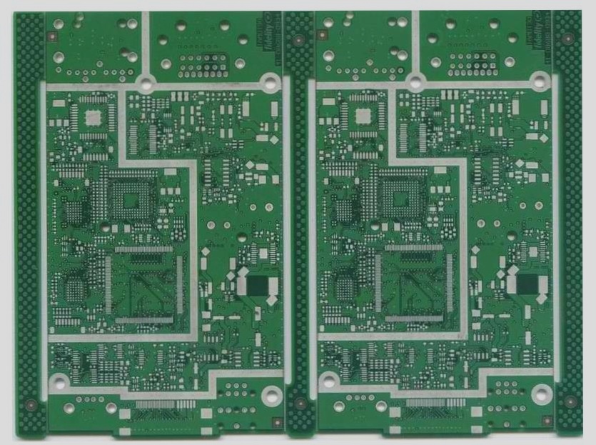
Design plays a critical role in the production of circuit boards. A well-thought-out circuit design is essential to ensure the final device functions correctly. Here are some key steps to follow in the PCB design process:
- Start with preliminary preparation, including creating component libraries and schematics.
- Focus on PCB structure design, layout, wiring, and optimization.
- Regularly check the Design Rule Check (DRC) and structure for quality assurance.
- Pay attention to the placement of components for efficient connections.
- Consider the positioning of high-quality and heat-sensitive components.
- Place clock generators near devices using clock signals for optimal performance.
- Include decoupling capacitors for integrated circuits and discharge diodes for relay coils.
- Aim for a balanced, dense, and orderly layout for a professional finish.
During the PCB layout stage, ensure components are placed strategically according to the board size and mechanical requirements. Divide the board into different functional areas and consider the feasibility of production and installation. Neat and organized component placement not only enhances the board’s appearance but also simplifies the wiring process.
By following these best practices and paying attention to detail during the design process, you can create high-quality circuit boards that meet performance expectations and function effectively.