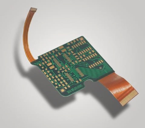
No matter how carefully you design a PCB, you will always find areas that can be improved upon once the design is complete. In general, it takes twice as long to optimize the routing compared to the initial wiring. Once you feel satisfied with the design, you can add copper layers (referred to as polygon planes). These copper layers are typically used for grounding (keeping analog ground separate from digital ground) and may also be necessary for power distribution on multilayer boards. When it comes to silk screen printing, be mindful of avoiding obstruction by components or removal by vias and pads. Additionally, always consider the orientation of components when designing, ensuring that the text on the bottom layer is mirrored to prevent confusion.
After ensuring the correctness of the circuit schematic design, it is important to physically connect the PCB layout file to the schematic for a network check. Any necessary revisions should be made promptly based on the results to ensure the accuracy of the connections.
Once the network check is successfully completed, the PCB design should undergo a Design Rule Check (DRC). Again, any required changes should be made based on the results to ensure the electrical performance of the PCB routing. Finally, it is essential to thoroughly review and confirm the mechanical installation structure of the PCB.
It is advisable to have a review process in place before finalizing the design. PCB design requires careful attention to detail, precision, and a high level of concentration. Only through meticulous work, a pursuit of perfection, and the accumulation of experience can a high-quality board be produced.
WellCircuits Limited specializes in manufacturing high-precision double-sided, multi-layer, impedance-controlled, blind/buried vias, and thick copper circuit boards. Our product range includes HDI, thick copper, backplanes, rigid-flex combinations, buried capacitance/resistance, Golden Finger, and other types of circuit boards to meet the diverse needs of our customers.


