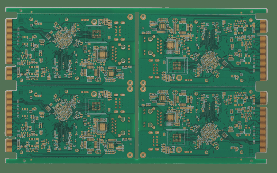
The copper cladding of a PCB board is a crucial step in PCB design, with significant technical content. Our senior engineers have discussed and summarized the following key points on how to approach the design work of this step.
Introduction of Copper Cladding:
Copper cladding involves using the unused space on the PCB as a reference surface and filling it with solid copper, also known as copper filling. The purpose of copper coating is to reduce ground wire impedance, improve anti-interference capabilities, decrease voltage drop, enhance power supply efficiency, and minimize loop area by connecting to the ground wire. Additionally, to prevent PCB deformation during soldering, most manufacturers require PCB designers to fill open areas with copper or grid-like ground wires. Failure to properly handle the copper can lead to various issues.
It is well known that under high-frequency conditions, the distributed capacitance of the wiring on a printed circuit board can cause issues. When the length exceeds 1/20 of the corresponding wavelength of the noise frequency, an antenna effect occurs, leading to noise emission through the wiring. Improperly grounded copper pours can exacerbate this issue, causing the copper to inadvertently spread noise. In high-frequency circuits, simply connecting the ground wire to the ground is insufficient. Proper handling, like ensuring connections are less than λ/20 and utilizing through holes in the wiring, is necessary for effective grounding. When done correctly, copper coating not only facilitates current flow but also shields against interference.
In copper coating, certain considerations must be taken into account to achieve the desired effects:
1. If the PCB features multiple grounds such as SGND, AGND, GND, etc., it is essential to use the main “ground” as a reference for independent copper pouring, distinguishing between digital and analog grounds. Prioritize thickening corresponding power connections like 5.0V, 3.3V, etc., before the copper pour to form multiple structured shapes.
2. For single-point connections of different grounds, utilize 0 ohm resistors, magnetic beads, or inductance for connection.