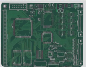
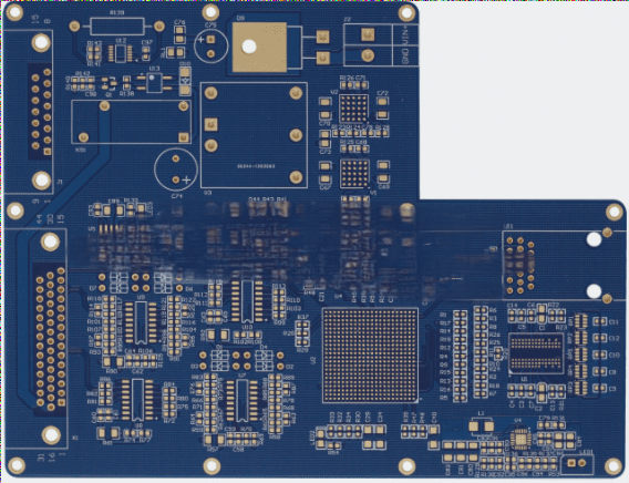
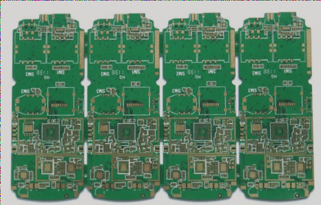
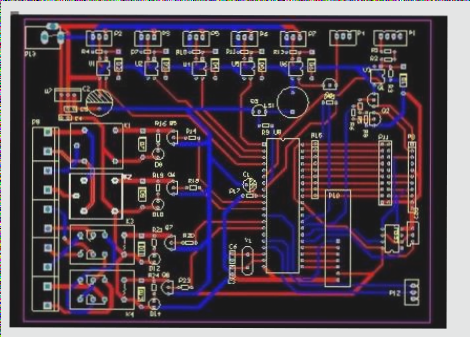
1. Upon receiving the bare PCB board, begin with a visual inspection to check for issues such as short circuits or open circuits. Next, familiarize yourself with the development board’s schematic diagram and compare it against the PCB’s screen layer to ensure consistency between the two.
2. Once you have gathered all necessary materials for PCB soldering, categorize the components by size to streamline the soldering process. It’s essential to print a comprehensive materials list. During the soldering phase, if an item remains incomplete, mark it with a pen to cross out the corresponding option, making future soldering operations more efficient.

1. Before welding, implement anti-static measures such as wearing a static ring to prevent damage to components from static electricity. Once the necessary equipment for welding is prepared, ensure that the soldering iron tip is clean and well-maintained. It is advisable to use a flat-angle soldering iron for the initial soldering. When working with components like 0603 packages, this type of soldering iron provides better contact with the pads, facilitating the soldering process. Of course, this may not pose a challenge for experienced professionals.
2. When selecting components for soldering, adhere to an order from small to large and low to high. This approach prevents smaller components from being affected by the soldering of larger ones. Priority should be given to soldering integrated circuit chips.
3. Prior to soldering the integrated circuit chip, confirm that the chip’s placement direction is correct. On the chip’s silkscreen layer, rectangular pads typically indicate the starting pins. Begin by securing one pin of the chip, then fine-tune the component’s position, and fix the diagonal pin to ensure accurate alignment before proceeding with soldering.
4. SMD ceramic capacitors and voltage stabilizing diodes do not have polarity in voltage stabilizing circuits. However, light-emitting diodes, tantalum capacitors, and electrolytic capacitors require careful attention to positive and negative terminals. For capacitors and diode components, the marked end usually indicates the negative terminal. In SMD LED packages, the direction of the lamp indicates the positive-negative orientation. For packaged components with a diode circuit diagram indicated by silkscreen, the diode’s negative end should be positioned at the end marked with a vertical line.
5. For crystal oscillators, passive types generally feature only two pins with no polarity distinction. Active crystal oscillators typically have four pins, so be sure to check the pin definitions to avoid soldering mistakes.
6. When soldering through-hole components, such as those related to power modules, the device pins can be adjusted before soldering. After placing and securing the components, the solder is usually melted from the back with a soldering iron and then flows to the front pad. It’s important not to use excessive solder, but ensure that the components are stable first.
7. Any PCB design issues encountered during the soldering process should be documented promptly. This includes installation interference, incorrect pad sizes, component packaging errors, etc., for future improvements.
8. After completing the soldering, use a magnifying glass to inspect the solder joints for any signs of cold soldering or short-circuiting.
9. Once the circuit board soldering is finished, clean the surface of the board with alcohol or other cleaning agents. This helps to eliminate any iron filings that may cause short circuits while ensuring that the board looks cleaner and more aesthetically pleasing.
2. Once you have gathered all necessary materials for PCB soldering, categorize the components by size to streamline the soldering process. It’s essential to print a comprehensive materials list. During the soldering phase, if an item remains incomplete, mark it with a pen to cross out the corresponding option, making future soldering operations more efficient.
1. Before welding, implement anti-static measures such as wearing a static ring to prevent damage to components from static electricity. Once the necessary equipment for welding is prepared, ensure that the soldering iron tip is clean and well-maintained. It is advisable to use a flat-angle soldering iron for the initial soldering. When working with components like 0603 packages, this type of soldering iron provides better contact with the pads, facilitating the soldering process. Of course, this may not pose a challenge for experienced professionals.
2. When selecting components for soldering, adhere to an order from small to large and low to high. This approach prevents smaller components from being affected by the soldering of larger ones. Priority should be given to soldering integrated circuit chips.
3. Prior to soldering the integrated circuit chip, confirm that the chip’s placement direction is correct. On the chip’s silkscreen layer, rectangular pads typically indicate the starting pins. Begin by securing one pin of the chip, then fine-tune the component’s position, and fix the diagonal pin to ensure accurate alignment before proceeding with soldering.
4. SMD ceramic capacitors and voltage stabilizing diodes do not have polarity in voltage stabilizing circuits. However, light-emitting diodes, tantalum capacitors, and electrolytic capacitors require careful attention to positive and negative terminals. For capacitors and diode components, the marked end usually indicates the negative terminal. In SMD LED packages, the direction of the lamp indicates the positive-negative orientation. For packaged components with a diode circuit diagram indicated by silkscreen, the diode’s negative end should be positioned at the end marked with a vertical line.
5. For crystal oscillators, passive types generally feature only two pins with no polarity distinction. Active crystal oscillators typically have four pins, so be sure to check the pin definitions to avoid soldering mistakes.
6. When soldering through-hole components, such as those related to power modules, the device pins can be adjusted before soldering. After placing and securing the components, the solder is usually melted from the back with a soldering iron and then flows to the front pad. It’s important not to use excessive solder, but ensure that the components are stable first.
7. Any PCB design issues encountered during the soldering process should be documented promptly. This includes installation interference, incorrect pad sizes, component packaging errors, etc., for future improvements.
8. After completing the soldering, use a magnifying glass to inspect the solder joints for any signs of cold soldering or short-circuiting.
9. Once the circuit board soldering is finished, clean the surface of the board with alcohol or other cleaning agents. This helps to eliminate any iron filings that may cause short circuits while ensuring that the board looks cleaner and more aesthetically pleasing.

