Effective Anti-ESD Measures in PCB Design
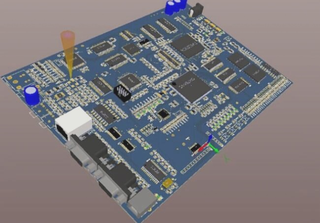
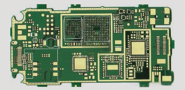
Implementing effective anti-ESD measures in PCB design is crucial to protect electronic components from damage caused by static electricity. By carefully layering, layout, and installation, ESD risks can be significantly reduced.
Key Strategies:
- Utilize multi-layer PCBs whenever possible to reduce common mode impedance and inductive coupling.
- Position components on both top and bottom surfaces with short traces for optimal performance.
- Employ tightly interwoven power and ground grids for double-sided PCBs.
- Keep circuits compact and connectors at the edges.
- Route power cords from the center of the card to minimize ESD vulnerability.
Additional Precautions:
- Place wide chassis ground beneath connectors prone to ESD impact.
- Connect mounting holes to chassis ground for added protection.
- Avoid soldering top or bottom pads during PCB assembly.
- Establish an isolation zone between chassis and circuit ground.
- Connect chassis ground and circuit ground near mounting holes for enhanced grounding.
By following these guidelines and implementing proper ESD protection measures, you can safeguard your electronic equipment from potential damage. If you require PCB manufacturing services, feel free to contact us.