Email:info@wellcircuits.com Phone: +86 191 4770 9860
1. **Minimize the Impact of Temperature on PCB Stress**

Since temperature is the primary factor influencing board stress, lowering the reflow oven temperature or slowing the heating and cooling rates within the oven can significantly reduce the likelihood of PCB bending and warping. However, other side effects, such as solder shorts, may arise as a result.

2. **Use High Tg Materials**

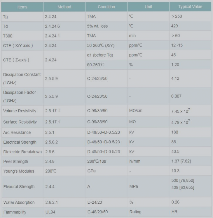
Tg (glass transition temperature) is the temperature at which a material shifts from a rigid glassy state to a more flexible, rubbery state. The lower the Tg, the faster the material softens in the reflow oven, and the longer it remains in a soft, rubber-like state, which can lead to greater deformation. Opting for higher Tg materials can improve the PCB’s ability to withstand stress and deformation, though these materials come at a higher cost.

3. **Increase PCB Thickness**

To meet the demands for lighter and thinner electronic devices, board thicknesses have been reduced to 1.0mm, 0.8mm, or even 0.6mm. Achieving sufficient rigidity and preventing deformation at these thinner thicknesses after reflow soldering can be challenging. If there is no specific requirement for thinness and lightness, it is recommended to use a board thickness of 1.6mm, which significantly reduces the risk of bending and deformation.

4. **Reduce PCB Size and Minimize Puzzle Cuts**


Since most reflow ovens use chains to advance the circuit board, larger circuit boards can experience denting and deformation due to their weight in the reflow furnace. To minimize this, it’s recommended to position the longer side of the circuit board along the edge of the chain. This helps reduce the depression and deformation caused by the board’s weight during the reflow process. The reduction in the number of panels is also a result of this approach. In other words, when passing through the furnace, it’s best to orient the circuit board with its narrow edge facing the direction of travel to minimize any potential deformation.

5. **Use of Furnace Tray Fixtures**

If the above methods are difficult to implement, the alternative is to use a reflow carrier or template to reduce deformation. The reason these carriers help minimize bending is that they support the circuit board during thermal expansion or contraction. The tray holds the board in place until its temperature drops below the Tg (glass transition temperature), at which point it begins to solidify, maintaining its original size and shape.

If a single-layer PCB pallet isn’t enough to prevent deformation, adding a cover to clamp the circuit board between upper and lower pallets can significantly reduce warping during reflow. However, this solution is relatively costly, and manual labor is required for placing and retrieving the trays.

6. **Use Router Instead of V-Cut for Sub-Boards**

V-Cuts can compromise the structural integrity of the board between individual circuit boards, so it’s best to avoid using V-Cuts for panel separation or to reduce the depth of the V-Cut when possible.

If you have any PCB manufacturing needs, please do not hesitate to contact me.Contact me