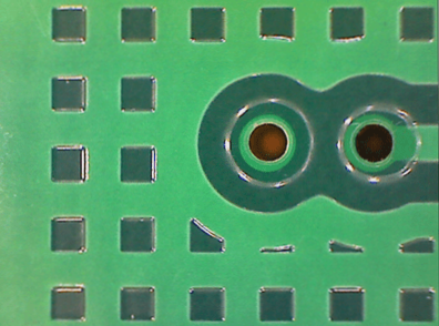
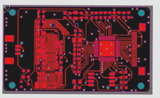
In the study of circuit board reverse engineering, the reverse push principle diagram refers to extracting the schematic from PCB documentation or directly creating a PCB circuit diagram based on the actual product. This process aims to elucidate the principles and operational conditions of the circuit board. Additionally, this circuit diagram is utilized to analyze the functional characteristics of the product itself. In forward design, typical product development begins with schematic design, followed by circuit board design based on the schematic.
Whether used for analyzing circuit board principles and product operational characteristics in reverse engineering or serving as the foundation for PCB design in forward engineering, PCB schematics hold significant importance. Therefore, how can one effectively reverse-engineer the PCB schematic based on documentation or the physical product? What key details should be considered during the reverse calculation process?
1. **Reasonably Divide Functional Areas**
When conducting the reverse design of a well-crafted PCB circuit board schematic, a logical division of functional areas can assist engineers in minimizing unnecessary complications and enhancing drawing efficiency. Generally, components with similar functions on a PCB are arranged in close proximity. This functional area division provides a convenient and precise reference when reversing the schematic diagram.

1. However, the division of functional areas is not arbitrary. It necessitates that engineers possess a solid understanding of electronic circuit principles. First, identify the core component within a specific functional unit, and then, by following the wiring connections, other components within the same functional unit can be located to create a functional partition. The establishment of these functional partitions serves as the foundation for schematic drawing. Additionally, during this process, it’s important to cleverly utilize the serial numbers of components on the circuit board, as they can expedite functional partitioning.
2. Correctly distinguish lines and design wiring appropriately.
When distinguishing between ground wires, power wires, and signal wires, engineers need relevant knowledge of power supplies, circuit connections, and PCB wiring. The differentiation of these lines can be assessed based on component connections, the width of the copper traces, and the characteristics of the electronic product itself.
In wiring diagrams, to avoid line crossings and overlaps, numerous grounding symbols can be employed for the ground lines. Different colors and line types can be used for various connections to ensure clarity and distinguishability. For different components, special symbols can be utilized, or even separate unit circuits can be drawn and later combined.
3. Identify the correct reference components.
The reference component can be considered the primary component utilized at the onset of schematic drawing. Once the reference component is established, the schematic can be drawn based on the pins of these components, enhancing the accuracy of the schematic.
For engineers, selecting reference components is typically straightforward. Generally, the components that play a crucial role in the circuit are chosen as reference parts. These components tend to be larger and have more pins, making them easier to work with. Integrated circuits, transformers, and transistors are all suitable candidates for reference components.
4. Understand the basic framework and learn from similar schematics.
Engineers should be well-versed in the composition of basic electronic circuit frameworks and the principles of drawing them. This proficiency allows them not only to draw simple and classic unit circuits but also to construct the overall framework of electronic circuits.
Moreover, it’s important to recognize that similar types of electronic products often share schematic similarities. Engineers can leverage their accumulated experience and draw insights from analogous circuit diagrams to inform the schematic design of new products.
5. Review and optimize.
Once the schematic drawing is complete, the reverse design process of the PCB schematic can be considered finished following thorough testing and verification. It’s essential to check and optimize the nominal values of components that are sensitive to PCB layout parameters. The schematic diagram should be compared and analyzed against the PCB file diagram to ensure complete consistency between the two.


