PCB Design: Optimizing Component Layout for Efficiency and Performance
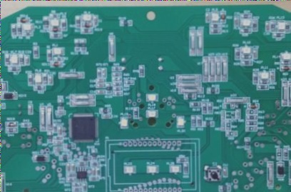
In the realm of electronic design, transitioning from schematic completion to PCB design marks a crucial phase. The initial steps involve defining fundamental aspects like board shape, size, and stack-up, setting the stage for component layout—the strategic placement of each element. This layout process holds significant importance, directly influencing routing quality and circuit performance. A well-executed layout not only kickstarts successful PCB design but also ensures board functionality and efficiency.
Principles and Best Practices for PCB Component Layout
- Divide the circuit into functional modules for better organization.
- Separate analog and digital sections to reduce interference.
- Isolate high-frequency circuits from low-frequency ones.
- Strategically place key components to guide overall layout.
- Pay special attention to routing sensitive circuits to avoid signal integrity issues.
- Consider electromagnetic compatibility (EMC) to minimize interference.
Common Challenges in PCB Layout
- Poor routing leading to signal degradation and complexity.
- Inadequate isolation between high-speed and sensitive components causing noise problems.
- Decoupling capacitors or grounding issues affecting power integrity.
- Thermal management oversights resulting in hotspots and potential failures.
- Striking a balance between compactness and signal integrity for efficient design.
Optimizing PCB Design for Functionality and Aesthetics
A successful PCB design not only meets performance standards but also boasts visual appeal and organization. Addressing key questions during the layout process is crucial for optimal performance, including considerations like board shape, component arrangement, and management of heat dissipation, signal integrity, and EMI.
Key Design Considerations and Challenges
1. Component Layout and Placement:
- Ensure specific cutouts or process edges are incorporated if needed.
- Reserve mounting and positioning holes appropriately.
- Optimize component spacing for efficient routing and performance.
- Address conflicts in height or level, especially with taller components.
- Integrate PCB shape with the overall machine design seamlessly.
2. Impedance Control and Signal Integrity:
- Maintain impedance control for high-speed signals.
- Stabilize the power delivery network (PDN) for reliable power signals.
Thermal Management for High-Power Components
- How to effectively manage heat dissipation for high-power components?
- Is the distance between thermal and heating elements appropriately considered?
EMC and Interference Mitigation
- Ways to enhance PCB layout for better electromagnetic compatibility (EMC) and noise reduction?
- Are components requiring frequent replacement easily accessible?
Principles for Optimal PCB Layout
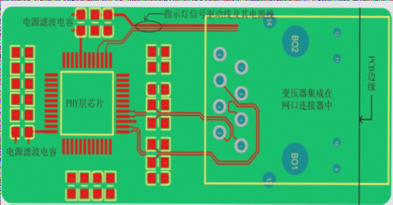
1. Functional Area Division
Start by dividing the PCB into functional areas to streamline signal flow and minimize routing complexity. Key areas like power supply, core control, and signal input/output should be strategically positioned for improved efficiency.
- Power Supply: Typically placed along the PCB edge for reduced interference and simpler routing.
- Core Control: Centrally located to enhance connectivity between modules.
- Signal Input/Output: Positioned on either side of the core control section.
- Connectors: Should be near the PCB edge for easy external connections.
- Human-Computer Interaction: Consider ergonomic factors for user interface placement.
Arrange components in a grid-like pattern with parallel or perpendicular alignment for both functionality and aesthetics, ensuring a neat layout.
2. Centralized Core Component Layout
Centralize core components of each functional module, minimizing lead lengths, EMI, and routing complexity. Special components like high-frequency parts and heat-sensitive devices require careful placement.
- Adjustable Components: Place in accessible areas for easy adjustments.
- Thermal Components: Position near edges for optimal heat dissipation.
- EMI-Sensitive Components: Keep away from high-EMI areas and use EMI filters close to the source.
3. Thermal Management
Proper thermal management is vital for PCB performance. Place heat-generating components at edges for efficient cooling, especially in vertical installations to promote natural airflow.
4. Power Distribution and Grounding
Efficient power distribution ensures signal stability and noise reduction. Minimize loop areas between power and ground planes to enhance signal integrity.
- Power and Ground Lines: Match carefully to minimize noise.
- Separate Power and Signal Domains: Isolate high and low-frequency circuits to reduce interference.
5. Signal Path Optimization
Optimize signal routing for minimal distance and path length, particularly for high-speed signals. Separate analog and digital circuits to minimize noise.
- Analog and Digital Circuit Separation: Isolate to avoid noise coupling.
- Low-Level Signal Isolation: Keep sensitive signal lines away from high-power or high-frequency lines.
6. Component Accessibility and Serviceability
Consider maintenance and replacement ease during layout. Ensure components needing regular adjustments are easily reachable for technicians or users.
Summary of PCB Layout Best Practices
- Group related components for simplified signal routing and reduced interference.
Key Principles for Optimal PCB Design
- Efficient Design: Optimize component placement and minimize lead lengths for improved signal integrity and reduced EMI.
- Thermal Management: Address heat dissipation by strategically positioning heating elements and optimizing power distribution.
- Signal Integrity: Isolate high-frequency and low-frequency circuits to prevent interference and protect sensitive components.
- Ergonomics: Prioritize ease of use and serviceability by placing frequently accessed components in convenient locations.
Adhering to these guidelines ensures that PCB designs excel in performance, manufacturability, and reliability, all while maintaining a visually organized and functional layout.
If you have any inquiries regarding PCB or PCBA, please don’t hesitate to contact me at info@wellcircuits.com.