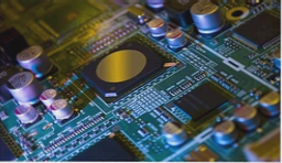
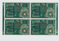
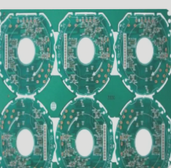
PCB Design Layout Concepts and Principles
Layout Concepts
When creating a PCB layout, it’s essential to consider the overall size of the PCB and the structural positioning of components. Pre-layout each circuit module based on signal and power flow direction, and then place components following the design principles of each module.
Basic Layout Principles
- Collaborate with stakeholders to meet structural, SI, DFM, DFT, and EMC requirements.
- Use structural diagrams to place key components with specific positioning needs.
- Designate no-route or no-layout zones based on component requirements.
- Balance PCB performance with manufacturing efficiency by selecting the appropriate process flow.
- Follow the pre-layout plan, placing large components first and then smaller ones.
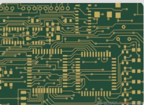
Ensure the layout minimizes wiring length, separates signal types, and maintains proper distances between components. Adopt a symmetrical, modular layout when possible.
- Use a 50 mil grid size for layout and a 25 mil grid for IC device placement.
- Minimize wiring length between FM components and increase spacing for devices with large voltage differences.
- Secure components heavier than 15g with brackets before soldering.
- Consider heat dissipation for components generating significant heat.
- Design adjustable components with mechanical requirements in mind.
Post-Layout Check
After completing the layout, verify PCB size markings, component alignment, and compliance with manufacturing process requirements.
PCB Design Checklist:
- Verify components do not interfere in 2D or 3D space or with the structural enclosure.
- Ensure all necessary components are placed correctly.
- Check accessibility of components that require frequent plugging or replacement.
- Confirm adequate spacing between heat-sensitive parts and heat-generating elements.
- Ensure easy access to adjustable components and buttons for operation.
- Verify unobstructed location for mounting heatsinks or radiators.
- Ensure smooth signal flow and minimize interconnection lengths.
- Consider potential signal interference issues.
- Check compatibility between connectors and mechanical design.
If you have any PCB manufacturing needs, feel free to contact us.