PCB Board Design Principles for Optimal Performance
Introduction
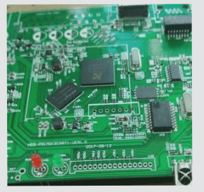
PCB boards play a crucial role in supporting circuit components and devices in electronic products by providing essential electrical connections. As technology advances, the density of PCBs continues to increase rapidly. Designing a high-quality PCB board is essential for its ability to resist interference and ensure optimal performance.
General Principles of PCB Board Design
- Consider component layout and wire placement carefully to achieve optimal electronic circuit performance.
- Follow general principles and meet anti-interference design requirements for efficient and cost-effective PCB board design.
Layout Considerations
When designing a PCB board, the size plays a critical role in its performance:
- Optimal size ensures proper impedance, noise reduction, and cost-effectiveness.
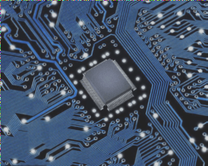
- Special components should be strategically located based on circuit functionality.
Special Component Placement Guidelines:
- Minimize connections between high-frequency components to reduce interference.
- Increase distance between components with high potential differences to prevent short circuits.
- Secure heavy components with brackets for stability and heat dissipation.
- Consider structural requirements for adjustable components like potentiometers and switches.
- Reserve space for printed pulleys and fixing brackets.
Component Layout Principles:
- Arrange functional circuits based on signal flow for efficient circulation.
- Center layout around each functional circuit element for a compact design.
- Align components in parallel for high-frequency circuits.
- Maintain proper spacing and aspect ratio for mechanical strength.
Wiring Guidelines
- Avoid adjacent or parallel wires at input and output terminals.
- Use appropriate wire width based on current value for optimal performance.
- Utilize arc-shaped corners for printed conductors in high-frequency circuits.
Pad and Line Design
Proper pad and line design are crucial for preventing virtual soldering and ensuring stability:
- Ensure pad center hole is slightly larger than the lead diameter.
- Adjust power line width based on current for reduced loop resistance.
- Separate digital and analog grounds for improved anti-noise capabilities.
By following these PCB board design principles, you can create efficient and high-performance electronic circuits with optimal anti-interference measures.
Decoupling Capacitor Configuration Tips:
- Place decoupling capacitors strategically on the PCB.
- Use an electrolytic capacitor across the power input and position ceramic capacitors close to IC chips.
- Connect decoupling capacitors directly to components sensitive to noise and voltage variations.
- Minimize lead wire length, particularly for high-frequency bypass capacitors, to enhance performance.
Latest Update: Research shows that using a combination of tantalum and ceramic capacitors for decoupling can further improve noise suppression and stability in PCB designs.