PCB Board Layout Operation Skills: Enhancing Power Quality and Anti-Interference Capability
- Principles of PCB Board Layout Operation Skills
- Importance of Filter Capacitors, Decoupling Capacitors, and Bypass Capacitors
- Optimizing Capacitor Placement for Effective Circuit Performance
Key Points to Consider:
- Decoupling capacitors and filter capacitors play a crucial role in power quality enhancement.
- Proper arrangement of capacitors improves the anti-interference capability of the circuit board.
- Inductance effects from traces and wiring in PCB design need to be addressed.
Operating Techniques for Effective PCB Design:
- Strategically place decoupling capacitors and filter capacitors near corresponding components.
- Use a 0.1μF decoupling capacitor to filter high-frequency ripple effectively.
- Position chip capacitors close to the power supply pins of components.
- Employ 10μF or larger capacitors for power conversion chips or input terminals to enhance power supply quality.
Best Practices for Component Layout and Routing:
- Mark footprints in the component library for easy identification.
- Print components at a 1:1 scale to verify sizes accurately.
- Utilize netlists from schematics with flying leads for efficient layout and routing.
- Avoid flipping components using X and Y keys to prevent soldering issues.
Design Considerations:
- Implement a layout strategy with horizontal lines on one side and vertical lines on the other for two-layer boards.
- Avoid placing unrelated vias near pads to prevent interference.
- Set design rules focusing on line width and spacing clearance for optimal performance.
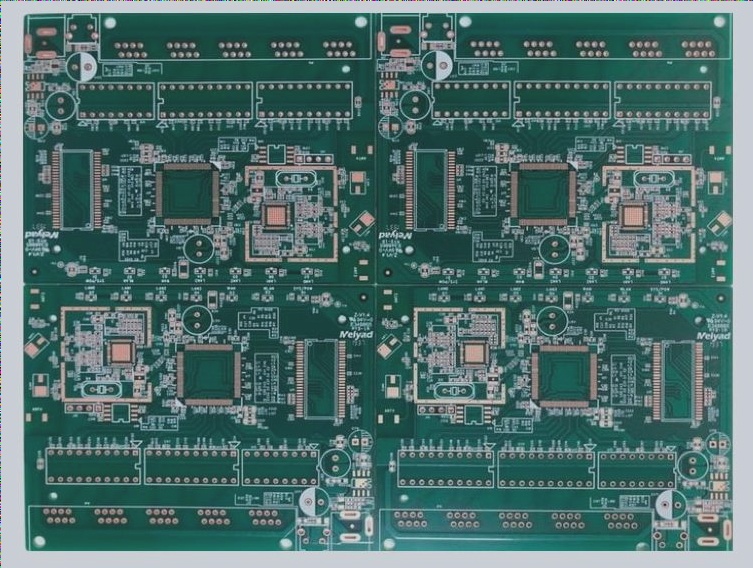
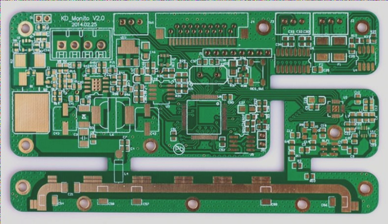
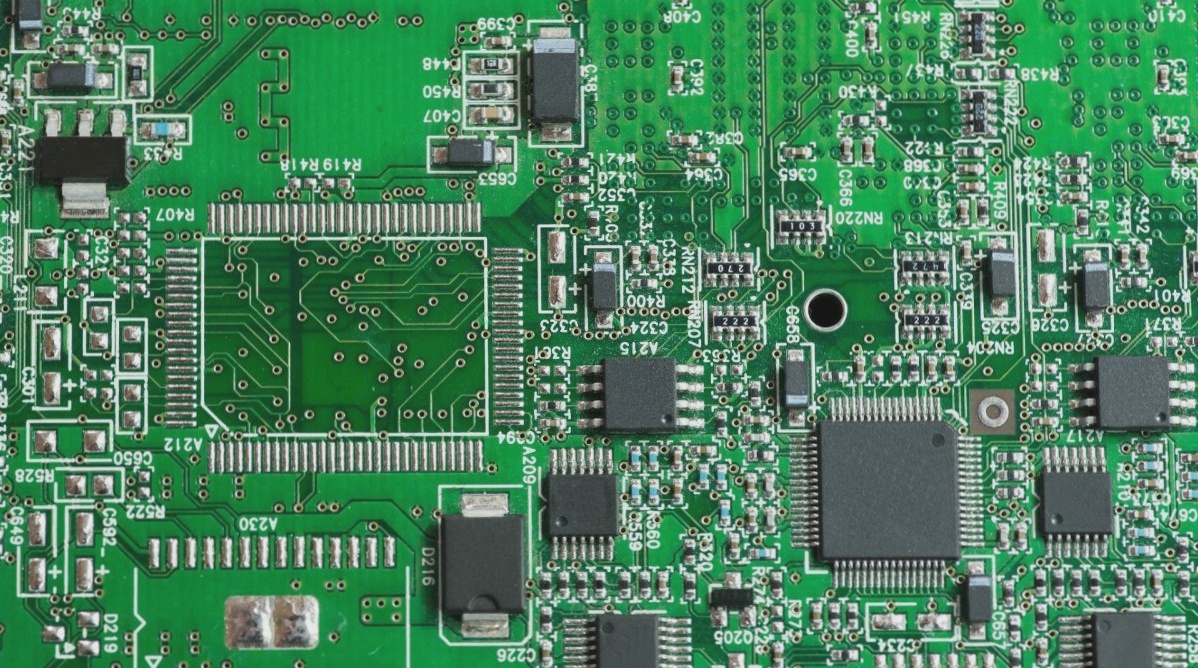
For a successful PCB design, understanding the functions and placement of filter capacitors, decoupling capacitors, and bypass capacitors is essential. These components not only enhance power quality but also improve the circuit’s anti-interference capability, ensuring stable operation and efficient performance.