Printed Circuit Boards (PCBs) and Effective Design Principles
Introduction to PCB Design and Importance
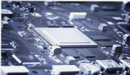
Printed Circuit Boards (PCBs) are crucial components in electronic devices, providing the foundation for circuit elements and electrical connections. As technology advances, PCB design quality becomes increasingly vital to minimize electromagnetic interference (EMI) and enhance electromagnetic compatibility (EMC).
Key Points in PCB Design
- Layout Optimization: Balancing performance, cost, and manufacturability is essential in PCB design. The size of the PCB impacts various aspects, and proper component placement is critical to ensure optimal performance.
- Component Placement Considerations: Strategic placement of components is crucial to minimize noise, interference, and maintain signal integrity. High-frequency components and sensitive parts require special attention.
Optimizing Component Placement
Efficient PCB design involves considering factors like trace length, component proximity, and interference sources. By following best practices, designers can enhance functionality and reliability.
Best Practices for Component Placement
- High-Voltage Components: Safety measures, such as maintaining safe distances between high-voltage components, are essential to prevent short circuits and ensure technician safety.
- Heavy and Thermal Components: Proper mounting and heat dissipation strategies are crucial for heavy components to prevent damage and maintain overall system performance.
- Adjustable Components: Positioning adjustable components strategically based on internal or external adjustments is vital for ease of use and maintenance.
- Positioning Holes and Brackets: Reserving space for mounting brackets and positioning holes is necessary for the overall structure and stability of the PCB layout.
Functional Circuit Layout Principles
Ensuring a logical circuit flow and signal direction is fundamental in PCB design to facilitate signal circulation and minimize interference, ultimately leading to efficient functionality.

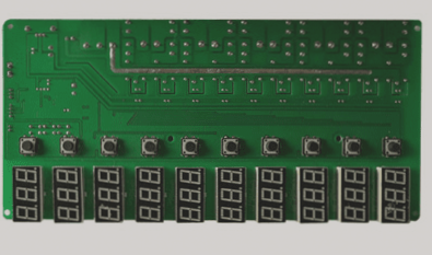
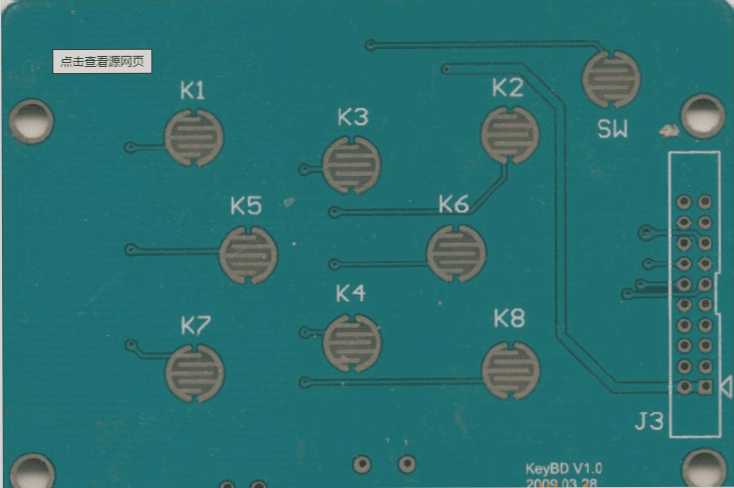
Centralized Component Arrangement
- Core components of each functional circuit should be centrally placed.
- Arrange other components around the core to minimize lead lengths and connections.
- Results in a more compact, efficient, and organized design.
High-Frequency Circuit Considerations
- For circuits operating at high frequencies, consider distributed parameters between components.
- Arrange components in parallel to improve aesthetics and ease of installation.
- Enhances soldering and mass production processes.
Edge Clearance
- Position components at least 2mm away from the PCB edges.
- Prefer a rectangular PCB with an aspect ratio of 3:2 or 4:3.
- For larger PCBs, consider mechanical strength to prevent warping or bending.
Wiring Principles
- Keep input and output wiring separate to avoid parallel routes.
- Add ground traces between signals to reduce feedback coupling.
- Consider wire width based on adhesive strength and current flow.
- Use wider traces for power and ground lines to improve current handling.
- Maintain appropriate trace spacing for insulation resistance and breakdown voltage.
- Avoid sharp right angles in traces for better electrical performance.
Pad Design
- Ensure the center hole of the pad is slightly larger than the component’s lead diameter.
- Pad’s outer diameter should be no less than (d + 1.2mm), where d is the lead diameter.
- For high-density digital circuits, the minimum pad diameter can be (d + 1.0mm).
PCB and Circuit Anti-Interference Measures
- Implement anti-interference design to ensure stable performance in noisy environments.
- Increase power trace width to reduce loop resistance and improve noise immunity.
- Align power and ground traces with data signal flow to reduce electromagnetic interference.
- Enhance overall noise suppression of the PCB.
By following these guidelines, your PCB layout will be efficient, safe, reliable, and optimized for manufacturing and performance.