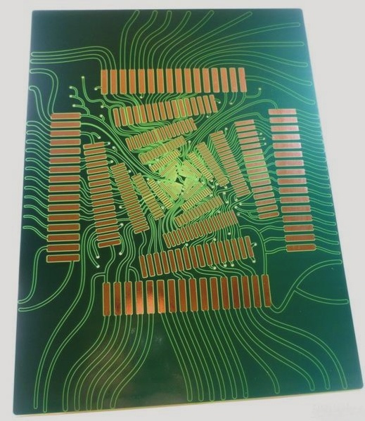
Printed Circuit Board Layout Principles
- Component Arrangement: Align components on the soldering surface according to the schematic diagram for easier testing and maintenance.
- Wiring Direction: Ensure wiring aligns with the circuit diagram for efficient production and inspection.
- Layout Distribution: Maintain a reasonable, even, and structurally strict distribution for a neat and beautiful appearance.
- Types of Placements:
- Horizontal Placement: Ideal for circuits with few components and a large board size.
- Vertical Placement: Suitable for boards with many components and a small size.
- Potentiometer Placement:
- IC Holder Usage:
For resistors, the distance between pads varies based on their power rating.
The distance between pads in vertical placement is generally 1 to 2/10 inches.
Potentiometers should be positioned on the board edge with the handle facing outward for easy adjustment of output voltage.
Ensure correct orientation and pin placement when using an IC holder. The first pin should align with the positioning groove on the soldering surface.
Latest PCB Design Trends
- Miniaturization: With the demand for smaller electronic devices, PCB designs are focusing on compact layouts and components.
- High-Speed Design: To meet the requirements of modern electronics, PCBs are being designed to support high-speed data transfer and processing.
- Flexible PCBs: Flexible printed circuit boards are gaining popularity due to their ability to conform to different shapes and spaces.
- Embedded Components: Integrating components within the PCB layers is a growing trend to save space and improve performance.