Printed Circuit Board (PCB) Design: Optimizing Performance and Anti-Interference
Introduction to PCB Design
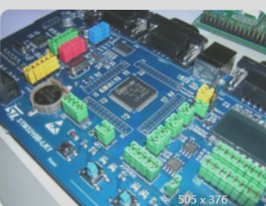
Printed circuit boards (PCBs) are crucial components in electronic products, providing support and electrical connections for circuit elements and devices. With advancing technology, PCB density has increased, emphasizing the importance of high-quality design to resist interference.
Key Principles for PCB Design
- Layout Considerations:
- Optimize PCB size to balance trace lengths, impedance, noise immunity, and costs.
- Minimize distance between high-frequency components to reduce interference.
- Space components to prevent short circuits and ensure safety.
- Secure heavy components for proper heat dissipation.
- Strategically position adjustable components for easy access.
- Arrange components based on signal flow and functional units.
- Consider distributed parameters for high-frequency circuits.
- Wiring Principles:
- Avoid running input and output wires parallel to reduce feedback coupling.
Effective PCB design enhances circuit performance and reliability, making it essential to follow these principles for optimal outcomes.
PCB Design Best Practices
-
Printed Trace Width and Spacing
The minimum width of printed traces is crucial for bond strength and current carrying capacity. For copper foil thickness of 0.05mm, a trace width of 1.5mm is recommended for optimal performance. Wider traces are preferred for power and ground connections. The spacing between traces depends on insulation resistance requirements and can be as small as 5–8mm for digital circuits.
-
Rounded Trace Corners and Copper Pour
Round corners of printed traces to improve electrical performance, especially in high-frequency circuits. Avoid large copper pours to prevent delamination under heat stress. If necessary, use a grid pattern to release volatile gases during heating.
-
Pad Design
Ensure the center hole of a pad is slightly larger than the component lead diameter to avoid poor soldering. The outer pad diameter should be at least (lead diameter + 1.2) mm, with a minimum of (lead diameter + 1.0) mm for high-density digital circuits.
-
PCB Noise Immunity Measures
Improving PCB noise immunity is crucial for overall performance. Key measures include:
-
Power Trace Design
Size power traces according to current requirements and align them with data lines for reduced loop resistance and enhanced noise immunity.
-
Ground Design Guidelines
Separate digital and analog grounds, use wide ground traces, and create closed loop ground circuits for improved noise immunity.
-
Decoupling Capacitor Configuration
Strategically place decoupling capacitors on the PCB to reduce noise. Consider capacitor values and placement for optimal performance.
-
If you require PCB manufacturing services, feel free to contact me.