PCB (Printed Circuit Board)
A Printed Circuit Board (PCB) is a crucial component in electronic devices, providing structural support and electrical connections between different electronic parts. The term “printed” originates from the process where conductive pathways are etched or printed onto a substrate, making it a vital element in modern electronics. PCBs are widely used in various devices, from simple gadgets like watches and calculators to complex systems such as computers, communication devices, and military technology.
Throughout history, early PCBs were crafted from paper-based copper-clad boards. However, the introduction of semiconductor transistors in the 1950s significantly increased the demand for PCBs. As electronic devices became more compact and intricate, especially with the emergence of integrated circuits (ICs), the necessity for advanced, high-density, and miniaturized PCBs grew. This progression has led to continuous innovation in PCB design and manufacturing techniques.
The development of PCBs has been fueled by the escalating requirements for higher circuit density, smaller form factors, and enhanced reliability. These advancements have resulted in PCBs with ultra-high density, miniaturization, and improved structural integrity. Additionally, new design approaches, specialized materials, and state-of-the-art fabrication techniques have surfaced to address the challenges posed by modern electronic applications.
Latest Updates:
- Emergence of 5G Technology: PCBs are playing a crucial role in the development and implementation of 5G technology, enabling faster data transmission and connectivity.
- Integration of IoT Devices: PCBs are being extensively used in the integration of Internet of Things (IoT) devices, facilitating seamless communication between connected devices.
- Advancements in Flexible PCBs: Flexible PCBs are gaining popularity due to their ability to conform to non-planar surfaces, opening up new possibilities for electronic designs.
Key Features of PCBs:
- Conductive Circuits
- Dielectric (Insulating) Layers
- Solder Mask (Solder Resist Ink)
- Silkscreen
- Surface Treatment
As the electronics industry continues to progress, PCBs are expected to evolve further, supporting increasingly complex electronic systems.

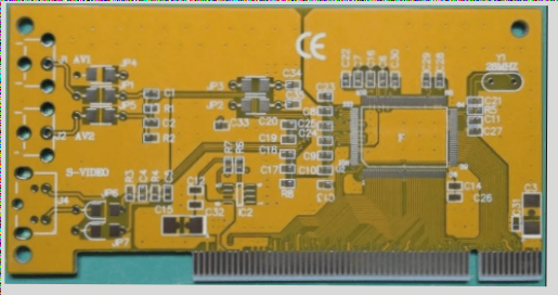
The appearance of a Printed Circuit Board (PCB) is commonly characterized by a green background, which is determined by the solder mask used during the manufacturing process. Additionally, a screen printing layer is applied to the solder mask, typically containing text and symbols to indicate component positions.
Advantages of PCBs:
- High Density: Development of high-density PCBs accommodates more components in smaller spaces.
- High Reliability: Rigorous testing ensures long-term reliability, suitable for various applications.
- Design Flexibility: Enables engineers to meet diverse requirements efficiently.
- Manufacturability: Standardized processes ensure consistent quality and cost-effectiveness.
- Testability: Comprehensive testing methods guarantee product quality and performance.
- Assemblability: Supports easy component assembly for efficient production.
- Maintainability: Facilitates maintenance and repair of electronic systems.
Advantages of PCBs in Electronic Systems
- Efficient Maintenance and Repair: Due to standardized components, quick replacement of faulty parts minimizes downtime.
Additional Benefits:
- Miniaturization and Lightweight: Compact design reduces system size and weight.
- High-Speed Signal Transmission: Supports fast electrical signals for high-performance devices.
- Reduced Wiring and Assembly Errors: Automated production minimizes human error.
- Circuit Interchangeability: Easier replacement or upgrade of parts.
- Facilitation of Equipment Miniaturization: Smaller, efficient designs reduce overall size.
- Production Automation: Enhances productivity and consistency.
In summary, PCBs provide essential advantages for modern electronic systems, improving performance, reliability, and efficiency in design and manufacturing processes.