PCB Assembly Process | Wellcircuits
Electronics are a crucial aspect of our everyday lives. Everything from our smartphones to our cars has electronic components. The heart of all electronics are printed circuit boards, often referred to as PCBs.
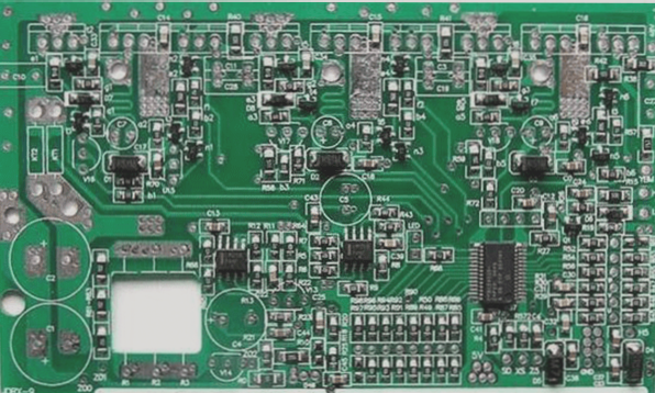
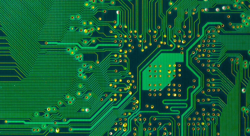
The majority of people are aware of printed circuit boards the moment they encounter them. They are the tiny green chips encased with copper lines you’ll find in the middle of electronic devices that are gutted. They are made of copper lines, fiberglass, and other metal components The boards are bonded by epoxy and then insulated with the use of a solder mask. The solder mask is where the distinctive green color comes from.
But, have you seen those boards that have components permanently attached? Don’t think of them as mere ornaments of a PCB board. A sophisticated circuit board won’t function until the components are mounted to it. A PCB with components mounted is known as the assembled PCB, and the process of manufacturing is known as PCB assembly. It’s also known as PCBA to shorten it. The copper lines on a bare board, also known as traces, connect electrical components and connectors. They transmit signals between these components, which allows PCBs to work in a specially developed manner. These functions vary from simple to the complicated however, the size of PCBs may be less than an inch.
How exactly are these devices constructed? The PCB assembly procedure is straightforward and is comprised of several manual and automated steps. Through each stage of the process each manufacturer offers an automated and manual option of which to pick. To help you comprehend the PCBA procedure from beginning to end, we’ve described each step in greater detail below.
PCB Design Basics
The PCBA procedure always begins with the simplest element of the PCB – the base composed of several layers. Each has a major impact on the performance that will be the end PCB. These layers alternate:
- Substrate: This forms the primary material used in PCB. It provides the PCB with its strength and rigidity.
- Copper A thin layer of copper foil that conducts electricity is added to every functional part of the PCB, either on one side, in the case of a single-sided PCB or both sides if it’s an asymmetric PCB. This is the copper layer that traces.
- Solder mask Over the copper layer is the solder mask that gives every PCB its distinctive green hue. It protects copper lines from accidental contact with other materials that conduct electricity that could cause the formation of a short. The solder, or the conductive material, will keep everything in its proper place. The holes within the mask are the places where solder is placed to join elements to the boards. A solder mask is an essential element for ensuring the smooth production of PCBAs because it prevents the process of soldering from occurring on components that should be avoided.
- Silkscreen: A silkscreen of white is the last layer on the PCB board. This layer provides labeling to PCB using symbols and characters. This allows you to identify the purpose of every part on the board.
The components and materials remain mostly identical across all PCBs apart from the substrate. The material used for the substrate of PCBs differs according to the particular qualities like cost and bendability every designer is seeking in the final product.
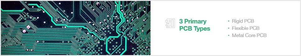
The three main PCB types are:
PCB Types | Wellcircuits
Rigid” PCB: The simplest PCB base type is a rigid PCB that is the basis for most PCBAs. Solid cores of PCB give the board its strength and thickness. The bases of PCBs that are inflexible consist of various substances. Most commonly, it is fiberglass, also known by the designation “FR4”. PCBs with lower costs are manufactured by using epoxies and phenolics, but they are less durable than FR4.
- Flexible PCBs Flexible PCBs provide some flexibility over their more solid counterparts. The material used in these PCBs is usually a flexible high-temperature plastic, similar to Kapton.
- PCB made of Metal Core The boards are another option to replace the traditional FR4 board. Built with a metal core, the boards are able to disperse heat more effectively than other. They help disperse heat and safeguard more sensitive components of boards.
Thru-hole technology | Wellcircuits
Two kinds of mounting techniques are prevalent in the present PCBA sector:

Surface Mount Technology Sensitive components, including some that are very tiny, like diodes or resistors, are put directly on top of the board. This is referred to as SMD assembly, which stands for surface mount devices. Surface mount technology is applied to small-sized components as well as integrated circuits (ICs). For instance, Wellcircuits is capable of mounting packages with a minimum. dimensions 01005. This is smaller than pencil points.
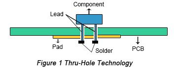
Thru-hole technology works on parts with wires or leads that have to be inserted into boards by plugging them into holes in the board. The lead component must be soldered to the opposite part of the board. This technique is used on PCB assemblies with big components like coils and capacitors that need to be joined.
Thru-hole technology | Wellcircuits
Due to differences between THT and SMT technologies, these must undergo different assembly processes and procedures. This article will address additional design and material considerations beyond the PCB’s core that are applicable to the assembly procedure concerning SMT, THT, and mixed technologies.
Before the Assembly Process
Some preparatory actions need to be taken before the real PCBA process can begin. This assists PCB makers assess the capabilities of the PCB design and usually involves the DFM assessment.
Many companies specializing in PCB assembly require the design file for the PCB to begin as well as any other design notes or specific specifications. This ensures that they PCB manufacturing company can examine on the PCB design file to identify any problems that could affect the PCB’s performance or manufacturing capabilities. The design is for manufacturing check, also known as a DFM check for short.
DFM Check | Wellcircuits
The DFM examination examines the specifications of the PCB’s design. Particularly, it looks for any redundant, missing or potentially dangerous features. These issues could significantly and adversely affect the overall functionality of the project. One example is that a common problem with PCB designs is the fact that there is insufficient space between PCB components. This could lead to problems with shorts, among others.
In identifying any potential issues before the manufacturing process begins, DFM checks can cut manufacturing costs and reduce unexpected costs. These checks reduce the number of boards that have been scrapped. In our dedication to quality and low expense, DFM checks come standard with every Wellcircuits project purchase. Wellcircuits offers free DFM as well as DFA check. However, they are worthless because the Valor’s DFM/DFA check Wellcircuits relies on an automated system that contributes to a high speed and accuracy.
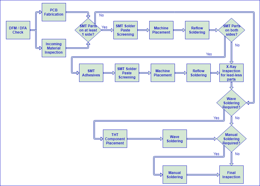
The actual PCBA procedure steps.
Step 1: Solder Paste Stenciling
The initial step in PCB assembly involves applying solder paste to the board. The process is similar to screen-printing a shirt; however, instead of masking, a thin stencil is applied to the PCB. This permits assemblers to apply solder paste to only certain components of the PCB they are planning to. These are the parts and the places where components will be placed on the final PCB.
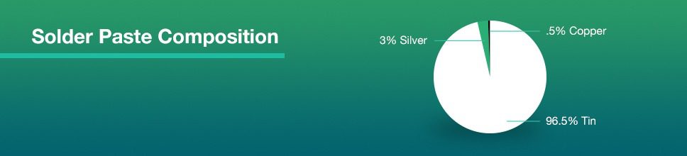
Solder Paste Composition | Wellcircuits
The solder paste is a gray substance that is made up of tiny pieces of metal. It is also referred to as solder. Its composition for these small metal balls is 96.5 percent Tin, 3% silver, and 0.5 percent copper. Solder paste blends solder and a flux, which is a substance that’s created to assist the melting of solder and adhere to the surface. Solder paste looks like a gray paste that must be placed on the board in precisely the right spots and in the exact quantities.
For a professional PCBA line an electronic fixture keeps the PCB and solder stencil in the correct position. The applicator is then able to apply solder paste over the planned areas with precise quantities. The machine distributes the paste over the stencil, spreading it evenly across each open area. When the stencil is removed you can see the paste remain in its designated locations.
Step 2: Pick and Place

Once the paste has been applied onto the PCB board which the PCBA process is moved to the pick-and-place machine. A robotic device puts surface mount components such as SMDs on a ready PCB. SMDs comprise the majority of PCBs that do not have connectors. They are then bonded onto the surface of the board during the subsequent stage of the PCBA procedure.
In the past, this was an manual procedure that was performed using an instrument called a tweezer, where assemblers were required to place and pick up components manually. Today, however this is now an automated procedure for PCB makers. This is due in large part to machines are generally more precise and reliable than human beings. While humans are able to work fast but fatigue and eye strain tend to take hold after a short period working with these small parts. Machines can work all day without fatigue.
Surface Mount Technology | Wellcircuits
The robot begins the pick-and-place process by grabbing PCB boards with an air grip and then shifting it to the station for pick and place. The robot will then position the PCB on the station before applying the SMTs onto the PCB’s surface. The components are then placed over the soldering paste in preprogrammed positions.
Step 3: Reflow Soldering
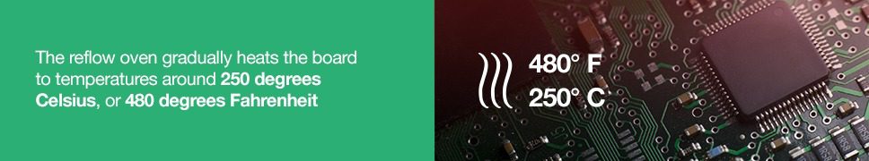
After the solder paste and components mounted on the surface are put in place, they have to stay there. That means that the solder paste has to be solidified by adhering the elements to the boards. PCB assembly achieves this by a process referred to as “reflow”.
When the pick and place process is complete and following the pick and place process, PCB board is then transferred onto the conveyor belt. The conveyor belt then moves through a large reflow furnace that is similar to a commercial pizza oven. This oven is made up of a set of heaters that gradually warm the board up to about 250 degrees Celsius, which is around 480 degrees Fahrenheit. It is enough heat for the melting of the solder within the paste of solder.
Reflow Soldering | Wellcircuits
When the solder is melted it, the PCB continues to pass across the oven. It is passed through a set of cooler heaters that permits the melted solder to be cooled and then solidify in a controlled fashion. This results in an permanent solder joint that will attach the SMDs onto the PCB.
A lot of PCBAs require particular consideration when reflowing, particularly in 2-sided PCB Assembly. Two-sided PCB assembly requires stenciling and reflowing every side individually. The first side that has fewer and smaller components is stenciled, positioned, and reflowed. Then comes the opposite side.
Step 4: Inspection and Quality Control

When the components for surface mounting are inserted into the board following the reflow process, this doesn’t mean the board is finished PCBA, and the board is required to be tested to ensure it’s functional. Most of the time, moving during the reflow process can result in poor quality connection or even a complete absence of connection. The shorts can also be a typical result of this process due to misplaced components that may connect parts within the circuits that are not supposed to connect.
Inspection and Quality Control Methods | Wellcircuits
Inspecting for these types of errors and misalignments may require the use of one or more inspection techniques. The most popular inspection methods are:
Manual checks: Despite the an upcoming trend toward automated and intelligent manufacturing, manual checks remain utilized in the PCB assembly. For small batches, an in-person visual inspection conducted by the designer is a reliable method to verify the quality of the PCB after the refining process. However, this technique becomes more difficult and ineffective when the number of examined boards grows. Examining such tiny components for longer than an hour can cause optical fatigue, which can result in less precise inspections.
Automated Optical Inspection Automated optical inspection is the most appropriate method to inspect large batches of PCBAs. A machine that is automated optical inspection is also known by the name of an AOI machine, employs an array of powerful cameras to “see” PCBs. These cameras are set at various angles to observe solder connections. Different solder connections of different qualities reflect light in various ways, which allows the AOI to identify a poor-quality solder. The AOI performs this task with great speed and can handle a large number of PCBs in a shorter period.
- X-ray Inspection: Another method of inspection is the use of x-rays. This is not the most frequent method of inspection — it is most commonly used for more intricate or PCBs that are layered. The X-ray lets a user view through layers and view lower layers to spot any hidden issues.
What happens to a board that is malfunctioning is contingent on the PCBA company standards. They are sent back to be cleaned and reworked or disposed of.
If an inspection reveals some of these issues and not. The next stage of the procedure is to check the part to ensure it’s doing what it’s intended to do. This is done by conducting tests on the PCB connections for quality. Boards that require programming or calibration need additional procedures to verify their functionality.
Regular inspections of the flow can be conducted after the reflow process has been completed to detect any possible issues. Regular inspections can guarantee that any errors are discovered and rectified as soon as possible. This helps both the manufacturer and designer to save time, effort and even materials.
Step 5: Through-Hole Component Insertion
Depending on the kind of board that is under PCBA the board could comprise a variety of components that go beyond SMDs. They include plated through-hole parts or PTH components.
A plated through-hole refers to an opening in the PCB that is completely plated throughout the board. PCB components make use of these holes to transfer the signal from one end of the circuit board to the opposite side. In this situation, it isn’t going to be of any use since the paste will go through the hole in a straight line without any chance of adhering.
Instead of using soldering paste, PTH components require a special type of soldering technique in the later stages of PCB assembly:
Manual Soldering: Hand through-hole insertion is an easy procedure. In most cases, a single person at one station will be responsible for inserting a particular component into a specified PTH. When they’re done, the board is moved into the station next, which is where a different person is tasked with inserting another component. The process continues for each PTH that needs to be equipped. It is a long procedure, based on the amount of PTH components that must be installed within a single cycle of PCBA. The majority of companies attempt to avoid using PTH components specifically for this goal, however, PTH elements are used within PCB designs.
*Wave Soldering soldering is an automated form of manual soldering. However, it requires a different method. After it is established that the PTH component is placed on the board, it is then placed on a different conveyor belt. This time the conveyor belt is pushed through a special oven, where the molten solder is sprayed over all the boards’ bottom. The process can solder all the pins that are on the top of the board in one go. This method of soldering is almost impossible on double-sided PCBs since it is impossible to solder the entire PCB side. could render delicate electronic components unusable.
Once the soldering process has completed, the PCB is ready to go through the final inspection or go through the process in case the PCB requires more components or another side assembly.
Step 6: Final Inspection and Functional Test
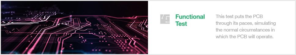
When the soldering phase of the PCBA process is completed, A final inspection is conducted to check the PCB for functionality. This is referred to as a “functional test”. The test tests the PCB through its paces by simulating typical conditions under which the PCB performs its function. Signals and power are simulated through the PCB during this test while the testers examine the PCB’s electrical performance.
Functional Test | Wellcircuits
When any one of the parameters like current, voltage, or output display unacceptable fluctuations or reach peaks that are outside of a specified range, then the PCB is not able to pass the test. The failing PCB is then able to be reused or destroyed, based on the specifications of the manufacturer.
Testing is the last and most crucial step in the PCB assembly as it is the determining factor in the success or otherwise of the procedure. Testing is the reason why periodic tests and checks throughout the process is vital.
After PCBA
Let’s just say that the PCB assembly is dirty. Soldering paste releases a small amount of flux, and the human hand can transfer dirt and oils from clothes and fingers onto the surface of the PCB. When all is said and done, the result may appear slightly dingy. This is both aesthetically pleasing and an issue of practicality.
After a while on a PCB, the flux residue begins to appear and smell as if it’s sticky. It also turns slightly acidic, which could cause damage to solder joints as time passes. Furthermore, customer satisfaction is likely to decrease when the shipments of brand-new PCBs are drenched with fingerprints and residue. This is why cleaning the product after completing the soldering process is essential.
A stainless-steel, high-pressure cleaning machine that makes use of diionized water can be the most effective method to remove the PCB’s residue. Cleaning PCBs with deionized water does not pose any danger to the equipment. This is due to the ions that are present in regular water that cause damage to circuits but not the water. Deionized water is safe for PCBs since they are subjected to a wash cycle.
Following washing, a short drying process using compressed air makes the PCBs ready to be packaged and shipped.
Differentialities between PCBAs: THT Assembly, SMT Assembly, and Mixed Technology
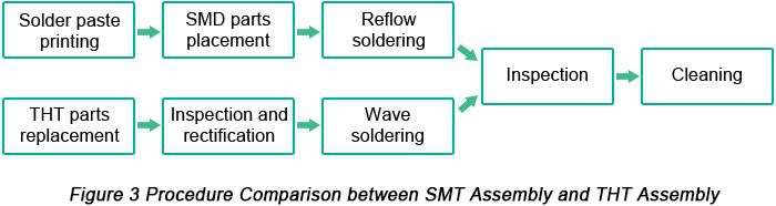
Comparing Procedures between SMT Assembly and Thru-hole Assembly | Wellcircuits
Thru-Hole Technology (THT) Assembly Process
As a standard PCB assembly method, the through-hole mounting is achieved by collaborating with manual procedures and automated processes.
- Components Positioning This process is completed manually by engineers who are professionals. Engineers must quickly and precisely place components in the same places based on the PCB design documents. The placement of components must be in line with the guidelines and operational requirements of the through-hole mounting processes to guarantee top-quality products at an affordable price. They have to determine the polarity and orientation of components to prevent operating components from impacting ambient components and to make the completed component placement in line with the corresponding standards, and wear anti-static wristbands with components that are sensitive to static, such as ICs.
- Inspection and Rectification The component placement has been completed. The board is placed into a suitable frame of transport where the components that are plugged into will be inspected automatically to see if they are properly put in. If any issues with the placement of components are found, it is easy to rectify them immediately, too. This is because it occurs prior to applying solder in the PCBA process.
- Wave Soldering – The components of the THT should be precisely soldered to the circuit board. With the wave soldering method, the board is moved across a swath of liquid solder that is heated to high temperatures, around 500 degrees F. Then, the board is soldered, all wires or lead connections can be made in order to ensure that the thru-hole components are secured with the boards.
Surface Mount Technology (SMT) Assembly Process
As compared to thru-hole mounting the surface mounting process stands out in terms of efficiency of production because it comes with an entirely automated mounting PCB assembly procedure that includes the printing of solder paste, to pick and place, as well as the reflow of soldering.
Step 1: Solder Paste Printing The process of printing Solder paste is applied to the board by the use of a solder paste printer. A template makes sure that solder paste will be precisely placed on the correct locations on the board where components will be placed It is also referred to as stencils or screens for soldering. Because the quality printed by solder is closely connected with the quality of soldering, PCBA producers that focus on top-quality products typically conduct inspections following solder paste printing with an inspector for solder paste. The inspection confirms that the printing met the requirements and standards. If any defects are discovered on the printing process, it needs to be repaired or the solder paste removed before the next printing.
The second step is Mounting Components – After removing the Solder paste printer, PCBs will be automatically sent to the pick-and-place machine, where components or ICs are mounted on the appropriate pads under the result of tension from the solder paste. Components are attached to the PCB board using component reels inside the machine. Similar to film reels, component reels containing components rotate to supply components to the machine, which can quickly adhere parts on the PCB board.
- Reflowing Soldering After each component has been placed, the board is passed through a 23-foot furnace. Temperatures of 500 degrees Celsius cause for the glue to become liquified. This is when the SMD components are firmly attached to the surface.
Mixed Technology
With the advancement of modern technological advancements, the electronic components become more complex that are driving complex smaller, more integrated PCB boards. It’s almost impossible to make PCBA’s that only have one type of component.
The majority of boards have SMD and through-hole components, which require cooperation between through-hole technology and SMD technology. However, soldering is a complex process that can be subject to a myriad of factors. This is why it is important to arrange the order of through-hole technology as well as surface-mount technology.
PCBA that makes use of mixed technologies must be implemented in the following scenarios:
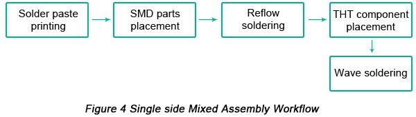
- Single Side Mixed Assembly Single-side mixed assembly adheres with the manufacturing method. Note: Hand soldering may be used instead of wave soldering if just a small quantity THT components is needed in this type of assembly.
Single-side Mixed PCB Assembly Workflow | Wellcircuits
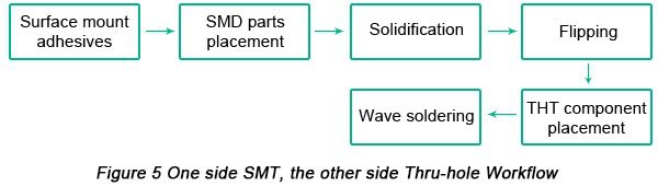
- One Side THT and THT on the other side: Take note that this type of PCB assembly process is not recommended as adhesives can increase the cost of PCBAs and could result in some soldering issues.
A side with SMT. The other Process of Thru-hole Assembly | Wellcircuits
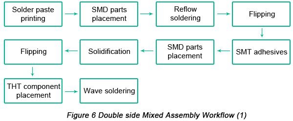
- Double Side Mixed Assembly: In regards to double side mixed assembly, two options PCBAs use adhesives, and PCBA that is not. Adhesives are used to increase the price of the PCB. Additionally, during the PCBA process, the heating needs to be conducted at least three times, which can cause lower efficiency.
Double side mixed PCB Assembly workflow | Wellcircuits
Double-side Multi-sided PCB Assembly workflow | Wellcircuits
Based on the analysis of mixed assembly methods discussed earlier, we can conclude that hand soldering is a good choice when PCB assembly requires numerous parts on each side of the SMD component, which is much more than the THT component. In situations where only a small amount of THT components are required, then it is the use of wave soldering is recommended.
PCB assembly must go through a complex and technical process in which many components must be considered, and even a minor change can result in a huge impact on the price and quality of the product. The descriptions of PCB assembly in this article will focus on standard PCBA methods and processes. The manufacturing process in practice is mostly controlled and influenced by design documents and the particular specifications of the customer. Therefore, evaluating the reliability of a PCB assembler is a critical issue that customers must think about before placing their PCBA purchase.
PCBA Professionals
Wellcircuits is the most reputable PCB solutions supplier. We are able to meet your PCB needs, from sourcing parts to electronic assembly. We’ll assist you at every step and offer you complete knowledge and quality assurance.
Full Turnkey PCB Assembly Service | Wellcircuits
When you choose us to be your partner in a cooperative PCBA firm and partner with a provider that offers the top quality. Our PCB assembly services meet the highest quality benchmarks and follow IPC Class 3, RoHS, and ISO 9001:2008 certification standards. Furthermore, we can deal with any kind of PCB – single-sided or double-sided or an SMT, through-hole or mixed-assembly projects. Whatever you’d like to do, you can have it happen!
We’ll stay in touch with you continuously from the start of the project right up until the end and keep you updated from design to assembly. This will help you save time and money with less PCB costs, shorter delays, and more high-quality products. We’re here to help you save time and energy so that you are able to focus only on the PCB designs without worrying about the details of manufacturing.
Start an Instant Quote for PCB Assembly
For more information on Electronic Assembly and what Wellcircuits can bring to the next PCB project, have a look at these pages:
- A Comprehensive Introduction to PCBAs
- How to Evaluate PCB Assembly Houses?
Wellcircuits offers Advanced Turnkey PCB Assembly Service without MOQ Requirement
- Design for Manufacture and Assembly of PCBs and General Rules It Conforms to
- Design PCBs to Better Take Advantage of Wellcircuits’ PCB Assembly Capabilities
- Instruction on Getting Precise PCB Assembly Prices