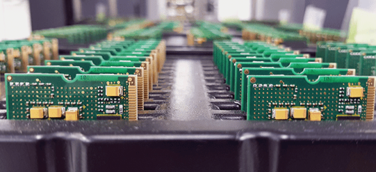
PCB Design Verification and Production Process

1. Design Conformance Check
- Verify spacings in customer’s design documents meet factory standards.
- Check trace width and via hole size for production feasibility.
- Ensure pad size and internal aperture integrity post-drilling.
2. Process Requirement Determination
Process parameters are set based on user specifications:
- Determine if light-painted negative requires mirroring for subsequent processes.
- Define solder mask expansion parameters to avoid errors.
- Consider key factors for solder mask expansion, including wire density and process lines.
3. CAD to Gerber Conversion
Standardize CAM process by converting CAD files to Gerber format. Maintain necessary process parameters during conversion for accuracy.
4. CAM Processing
Perform specified process treatments, paying attention to intricate details in user files.
5. Light Drawing Output
Utilize CAM-processed files for output using light drawing. Make necessary process adjustments for high-quality output.
6. Darkroom Processing
Develop and fix light-painted negative film in darkroom. Control development, fixing, and washing times to ensure quality output.
For more information on PCB fabrication, visit PCB.