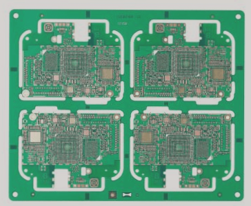
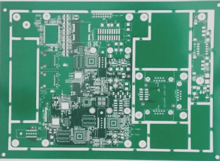
PCB Proofing Process: A Comprehensive Guide
As a leading PCB manufacturer, we specialize in SMT chip processing, circuit board proofing, and PCB board manufacturing. Our circuit board factory is committed to assisting everyone in understanding the PCB circuit board copying methods and proofing steps.
Step-by-Step Guide to PCB Proofing:
- Step 1: Prototype Acquisition
- Step 2: Component Removal and Cleaning
- Step 3: Layer Polishing and Scanning
- Step 4: Contrast and Brightness Adjustment
- Step 5: File Conversion to PROTEL Format
- Step 6: Conversion to TOP.PCB
- Step 7: Conversion to BOT.PCB
- Step 8: Image Integration in PROTEL
- Step 9: Printing and Verification
For multi-layer boards, additional steps are required, including meticulous polishing of inner layers and careful alignment verification.
Throughout the PCB proofing process, it is crucial to follow each step meticulously to ensure accuracy and efficiency.