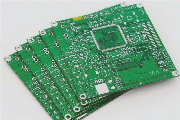
The base film of FPC is commonly composed of polyimide (abbreviated as PI) and polyester (PET). The material thickness ranges from 12.5 to 125 micrometers, with 12.5 and 25 micrometers being the most frequently used. When FPC requires soldering at high temperatures, polyimide (PI) is typically chosen, whereas FR4 is commonly used as the substrate for PCBs.
The cover layer of FPC is made from dielectric film, adhesive film, or flexible dielectric coatings to safeguard against contamination, moisture, scratches, etc. The primary material used is also polyimide, with typical thicknesses around 12.5 micrometers.
Designing FPC involves bonding these layers together, requiring the use of FPC adhesive (glue). Flexible boards typically employ adhesives such as acrylic, modified epoxy, phenolic butyral, reinforced plastics, or pressure-sensitive adhesives. In contrast, single-layer FPC does not necessitate adhesive bonding.

1. In many applications, such as welding devices, flexible boards require reinforcements for external support. Common materials include PI or polyester film, glass fiber, polymer materials, steel plate, aluminum plate, etc. PI or polyester film is frequently used for flexible board reinforcement, typically with a thickness of 125μm. Glass fiber (FR4) reinforced boards are harder than PI or polyester and are suitable for more demanding applications.
2. Various methods exist for handling FPC pad relative to PCB pad connections. Common methods include:
1. **Chemical Nickel Gold (ENIG):** Also known as chemical immersion gold or immersion gold. Typically, the electroless nickel layer thickness on the copper metal surface of the PCB ranges from 2.5μm to 5.0μm, and the immersion gold layer (99.9% pure gold) thickness ranges from 0.05μm to 0.1μm. Technical advantages include a smooth surface, long storage time, and ease of soldering, making it suitable for fine-pitch components and thinner PCBs. However, it is not environmentally friendly.
2. **Tin-Lead Electroplating:** Provides flat lead-tin directly on the pad, ensuring good solderability and uniformity. This method is essential for processes like HOTBAR on FPCs. Drawbacks include lead oxidation susceptibility, short storage time, the need for plating line adjustments, and environmental concerns.
3. **Selective Gold Electroplating (SEG):** Involves plating gold selectively on certain PCB areas after applying a nickel layer (2.5μm to 5.0μm thick). The gold layer thickness typically ranges from 0.05μm to 0.1μm. Advantages include enhanced oxidation and wear resistance, making it suitable for components like “Golden Fingers.” However, it poses environmental challenges due to cyanide pollution.
4. **Organic Solderability Protective Layer (OSP):** Covers the bare PCB copper surface with organic substances to achieve a flat surface meeting environmental standards. Suitable for PCBs with fine-pitch components but incompatible with traditional wave soldering and selective wave soldering processes.
5. **Hot Air Leveling (HASL):** Involves covering exposed PCB metal surfaces with a 63/37 lead-tin alloy layer (1μm to 25μm thick). Difficulties include controlling plating layer thickness and land pattern, making it unsuitable for fine-pitch components but suitable for thin FPCs.
3. In design, FPCs often complement PCBs, with various connections such as board-to-board connectors, connectors and golden fingers, HOTBAR, soft and hard bonding boards, and manual soldering employed based on application-specific requirements.
4. Environmental considerations prompt the selection of suitable connection methods, including the determination of whether ESD shielding is necessary based on application demands. When high FPC flexibility isn’t essential, solid copper and thick media suffice, whereas demanding flexibility requires specialized protection.
5. Due to FPC softness and susceptibility to pressure-induced damage, specific protective measures are necessary:
1. Ensure a minimum inner corner radius of 1.6mm on flexible profiles to enhance reliability and tear resistance. Adding a reinforcement line near board edges can prevent tearing.
2. Cracks or grooves in FPCs should terminate with round holes of at least 1.5mm in diameter, particularly when adjacent parts of the FPC need separate movement.
3. Opt for a uniform width bending area to enhance flexibility, avoiding variations in FPC width and trace density within bending regions.
4. Stiffeners (also known as stiffener boards) made from materials like PI, polyester, glass fiber, polymer, aluminum, or steel provide crucial external support. Thoughtful design of their placement, size, and material selection significantly reduces the risk of FPC tearing.
5. In multi-layer FPC designs, incorporate air gap layers in areas subject to frequent bending during product use. Using thin PI material enhances FPC flexibility, preventing cracking during repeated bending.
6. Designated double-sided tape fixing areas at joints between golden fingers and connectors help prevent detachment during bending.
7. Include FPC positioning screens at connections with connectors to ensure alignment during assembly and prevent skewing.
These edits aim to clarify and refine the original text while maintaining the integrity of its technical content.


