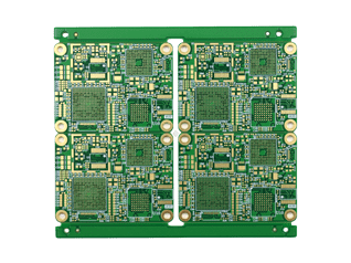
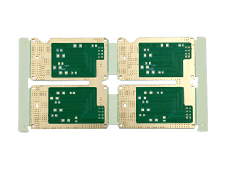
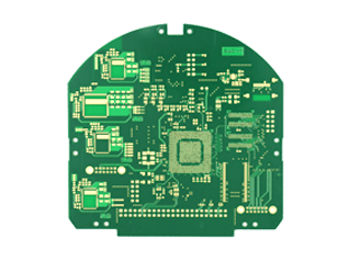
Product Material: FR-4 Shengyi S1000-2M,
Number of Layers: 16 layers,
Board Thickness: 1.80mm,
Surface Treatment: Gold immersion,
Line Width/Line Spacing: 3/3 mil,
Minimum Hole Diameter: Mechanical 0.15mm/Laser 0.10mm,
Technical Features: HDI seven-stage arbitrary stage
Home » Shop » PCB Fabrication » 16-layer HDI of any order
16-layer HDI of any order
**Product Details**
The 16-layer 7-step HDI arbitrary interconnection buried hole PCB is one of the HDI series circuit boards developed and produced by Qinlv Internation Co., Ltd. This 7-step HDI buried hole circuit board is made from Shengyi S1000-2M material, and formed through multiple laser drilling and lamination processes. It is widely used in high-end automotive main control servers, aerospace, and military industries. High-density interconnection HDI printed circuit boards (PCBs) play a crucial role in modern electronic devices, especially in applications requiring high signal transmission speeds and miniaturization.
Qinlv’s PCB technology team will delve into the ultimate technical characteristics, manufacturing process advantages, and challenges of the 16-layer 7-step HDI PCB featuring arbitrary interconnection buried holes.
1. **Introduction**
As electronic products evolve towards thinner and higher-performance designs, HDI technology has seen widespread application. The 16-layer 7-step HDI PCB developed by the Qinlv Wellcircuits PCB team features more layers and a more complex interconnection structure to meet the demands of high-end electronic devices. We will focus on the buried hole technology, which is key to achieving high-density interconnections.
2. **Technical Features**
2.1 **Layers and Steps**
The 16-layer 7-step HDI PCB refers to having 16 conductive layers, with interconnections made across at least 7 different layers. This structure provides more routing space and enables more complex circuit designs.
2.2 **Definition of Buried Holes**
A blind hole penetrates only part of the layers, while a buried hole is completely located within the board and does not penetrate the top or bottom layers. Buried hole technology increases interconnection density without adding to board thickness.
3. **Manufacturing Process**
3.1 **Drilling and Electroplating**
Micro-drilling technology is used to create buried holes between specific layers, followed by an electroplating process to form conductive layers on the hole walls for electrical connections between different layers.
3.2 **Lamination and Exposure**
Special lamination processes are employed to bond the layers together, followed by exposure and developing processes to create intricate circuit patterns.
3.3 **Surface Treatment**
Finally, surface treatment is conducted to protect the circuits from environmental impacts and enhance soldering performance.
4. **Advantages**
4.1 **High-Density Routing**
The buried hole technology allows for more routing layers within a limited space, significantly enhancing the integration level of the circuit board.
4.2 **Improved Performance**
By reducing the length of signal transmission paths, the 16-layer 7-step HDI PCB achieves lower latency and better signal integrity.
4.3 **Miniaturization**
The high number of layers and steps in HDI PCBs can significantly reduce the size of electronic devices, meeting the needs of portable equipment.
5. **Challenges**
5.1 **Manufacturing Difficulty**
The manufacturing process for 16-layer 7-step HDI PCBs is extremely complex, with high demands for process precision and consistency, increasing production difficulty and costs.
5.2 **Reliability**
The reliability of buried holes is a critical issue, especially in high-temperature and high-humidity environments. Ensuring the stability of the conductive layer on the hole walls and the reliability of connections poses a challenge.
5.3 **Design Complexity**
Due to the complexity of the layers and interconnection structures, designing a 16-layer 7-step HDI PCB requires consideration of more electrical and mechanical constraints, greatly increasing design difficulty.
6. **Conclusion**
The arbitrary interconnection buried hole technology in the 16-layer 7-step HDI PCB represents the highest level of the current electronic manufacturing industry. Despite facing numerous challenges, its advantages in high density, high performance, and miniaturization make it one of the key technologies for the future development of electronic devices. The Wellcircuits PCB team can further enhance its reliability and economic viability through continuous optimization of manufacturing processes and design methods.
SKU: cc772ea08d5d Categories: IOT & IIOT PCB, PCB Fabrication, Rigid PCB Tags: flex pcb, gerber viewer, PCBA, RF PCB
IOT & IIOT PCB, PCB Fabrication, Rigid PCB


