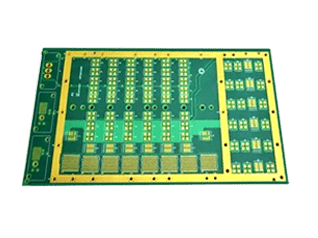
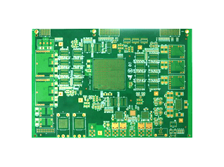
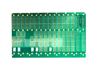
Number of layers: 22L,
Board thickness: 3.0+/-0.3mm,
Material: IT-968G,
Impedance: 36 groups,
Back drilling: 15 groups,
STUB capability: 0.15mm,
Hole to trace: 0.175mm
Home » Shop » PCB Fabrication » 22-Layer high-speed back drilling PCB
22-Layer high-speed back drilling PCB
Product Details
The 22-layer high-speed back-drilled PCB is a high-multilayer circuit board developed and manufactured by Shenzhen Jianxiangsheng Technology Co., Ltd.
This circuit board is made using IT-968G ITEQ high-speed laminate material, processed with surface treatments like gold immersion and back-drilling techniques.
The main technical features and challenges of this 22-layer high-speed back-drilled PCB are its advanced multi-layer back-drilling, which is widely used in fields such as communication, industrial internet control, and more.
PCB back-drilling technology is a manufacturing process mainly used in high-speed and high-density interconnect (HDI) PCBs. The core of this technology involves further drilling away unnecessary parts of the hole wall in already drilled through-holes (TH) or blind vias (BV), typically at one or both ends of the hole. The purpose of this is to improve signal integrity, reduce signal loss, and minimize interference during transmission.
In the manufacturing process of high-speed back-drilled PCBs, the back-drilling technology removes the stub segments of through-holes that do not play a role in connection or signal transmission, preventing negative effects on high-speed signal transmission. This method allows precise control of hole depth, removing only the unwanted metal portions without damaging surrounding traces.
The main advantages of back-drilling technology include:
– **Improved Signal Integrity**: By removing unnecessary metal sections along the signal path, back-drilling reduces signal reflection and scattering, enhancing transmission speed and quality.
– **Reduced Crosstalk**: Back-drilling helps minimize coupling between adjacent traces, lowering crosstalk and improving circuit performance.
– **Flexible Application in Multi-layer PCB Design**: Back-drilling is suitable for multi-layer PCB design, optimizing inter-layer connections by removing unwanted via segments.
– **Enhanced Thermal Performance**: Back-drilling can improve PCB thermal management by removing unnecessary metal, which helps in heat conduction and dissipation.
WellCircuits Qinlv’s high-speed back-drilled PCBs are processed using high-precision equipment and strict process control to ensure that the back-drilling depth and accuracy meet design specifications. Additionally, to guarantee the overall performance of the circuit board, back-drilling technology is typically combined with other high-speed PCB design and manufacturing techniques, such as selecting appropriate materials, optimizing routing layouts, and controlling impedance matching.
SKU: 21455ac9d72f Categories: PCB Fabrication, Rigid PCB Tags: flex pcb, gerber viewer, PCBA, RF PCB
PCB Fabrication, Rigid PCB


