6-layer TV Display PCB|wellcircuits high precision PCB | RF PCB
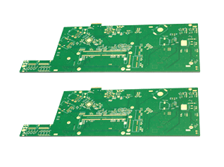
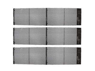
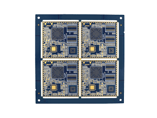
The 6-layer TV display board is a high multi-layer series circuit board developed and produced by Wellcircuits. This circuit board is made using high-quality IT-158 material, and is manufactured through processes such as laser drilling and gold plating on the surface. The main technical features and difficulties of this 6-layer TV display board are the ultra-long high-density gold fingers, high alignment accuracy, and it is widely used in the field of optoelectronics.
In TV display board PCBs, ultra-long high-density gold fingers can also be used for interfaces that require high-speed data transmission or high power supply, such as HDMI, DP, USB 3.0, and other high-speed interfaces or power interfaces. The design of these gold fingers needs to meet the following characteristics and requirements:
High signal integrity: To support high-definition video and high-speed data transmission, gold fingers need to have good signal integrity, which is usually achieved by controlling the impedance matching of the gold fingers, reducing signal reflection, and noise interference.
High current carrying capacity: For power interface gold fingers, they need to have a high current carrying capacity to support the high power requirements of display devices. At the same time, it is necessary to ensure low contact resistance to reduce energy loss and heat generation.
High durability: The interfaces on the TV display board may need to withstand frequent plugging and unplugging operations, so the gold fingers should have high wear resistance and corrosion resistance to ensure a long service life.
Precise alignment system: Due to the high density of the gold fingers, a precise alignment system is needed during the design to ensure that the interface plugs and sockets can be correctly aligned to avoid any possible damage or poor contact.
Compatibility and standardization: The design of the gold fingers must comply with relevant interface standards to ensure compatibility with other devices. At the same time, it is necessary to closely monitor the updates of the standards to support the latest devices and technologies.
In the production process, the processing of ultra-long high-density gold fingers requires the use of high-precision molds and advanced stamping techniques to ensure the accuracy of dimensions and shapes. Surface treatment processes are also very important, and gold plating or other corrosion-resistant, low contact resistance materials are usually chosen to ensure the electrical performance and service life of the gold fingers.


