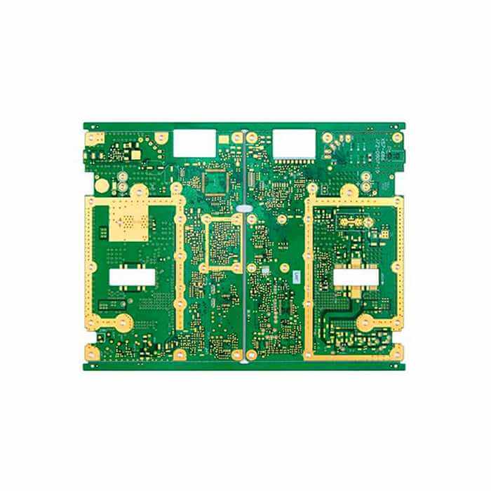
Layers : 8L
Thickness : 1.6mm
Out Layer Copper Thickness : 1 OZ
Inner Layer Copper Thickness :1 OZ
Min hole size :0.3mm
Min Line Width/Space: 5mil
Surface finish : ENIG
Application :Communication electronics and base station
Features : Mixed pressure
Get Instant Quote Now
WellCircuits ADVANTAGES
- In-house engineering
- Turnkey FPC & Assembly Solution
- Quick-turn up to 48hrs
- In-house assembly lines
- Support Prototype | Series Production


Reviews
There are no reviews yet.