Layers : 26L
Thickness : 6.6mm
Out Layer Copper Thickness : 2 OZ
Inner Layer Copper Thickness : 2 OZ
Min hole size :0.8mm
Min Line Width/Space : 3mil
Surface finish : Hard Gold
Application : IC testing instrument
Features : High complexity multilayer
WellCircuits™: Quick-Turn HDI PCB Prototype | Elic Elic HDI PCB Manufacturer
WellCircuits™ Description
WellCircuits is a PCB manufacturer dedicated to all sorts of HDI PCBs, including HDI flex PCB, rigid HDI PCB, rigid-flex HDI PCB. Among them, Rigid HDI PCB is the most common type. Our HDI PCBs are widely used in telcom, satellite, automotive, semiconductor and other high-end industries. Below are our basic capability:
- Layer: 2-36 layers, 1+5 Tiers
- Board size: 20”*35”
- Thickness: 0.2mm-6.0mm
- Impedance: 5%
- Min hole size: 0.076mm( Laser-drilled),0.15mm( Mechanical drill)
- Finish: HASL, HASL-LF, Gold Plating, OSP, Immersion Ag, Immersion Sn
- Expedited Service: 15hrs: double-sided; 24hrs: 4 layer; 36hrs: 6-8 layers; 60hrs: 10 layer; 72hrs:10 above
HDI PCBs Display
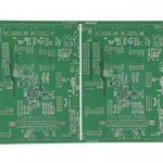
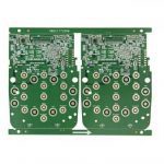

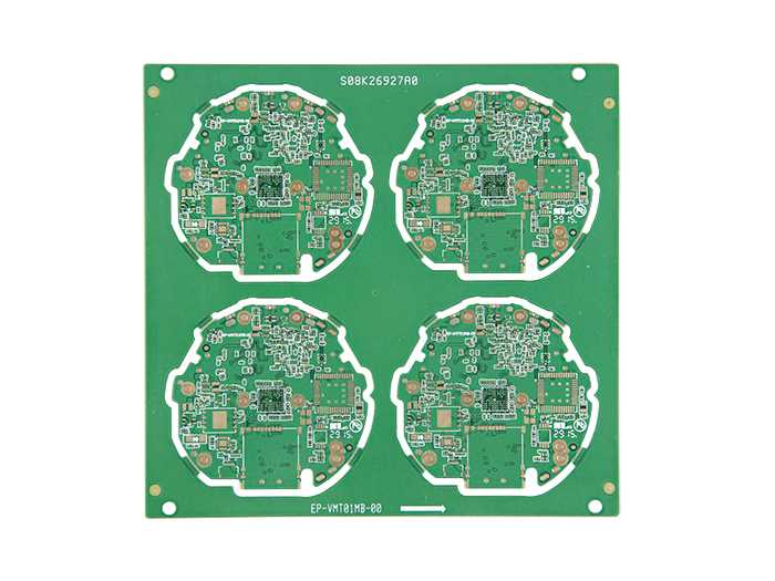
Layer:6L 2 Tier
Thickness:1.3mm
Size:118.29mm*113.12mm
Min blind vias:0.1mm
Min buried vias:0.2mm
Min Trace:0.084mm
Min Space:0.089mm
Finish:ENIG+OSP

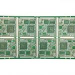
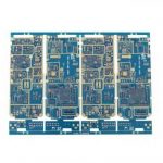
Layer:4L 1 Tier
Thickness:0.8mm
Size:70mm*86mm
Min Trace:0.12mm Min Space:0.075m
Min Hole Size:0.1m
Finish:ENIG+0SP
Application: Smart Watch

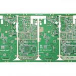
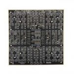
Layer:6L 2 Tier
Thickness:1.0mm
Size:92mm*118mm
Min Trace:0.075mm
Min Space:0.075mm
Min Hole:0.1mm
Finish:ENIG
Application: Mobile Phone
 Layer:8L 2 Tier
Thickness:1.0mm
Size:118.29mm*113.12mm
Min blind vias:0.1mm
Min buried vias:0.2mm
Min Trace:0.084mm
Min Space:0.089mm
Finish:ENIG+OSP
Application: Car DVR
HDI PCB Service
- Multi-layers HDI PCB(1-20L)
- Blind, buried and plugged vias
- 3 mil Trace/ 3 mil Space
- Max Panel Size 25"x17''
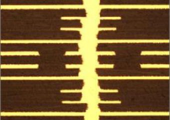
- ENIG, OSP, HASL-LF, Via Filling
- Smallest Hole Size: 0.1mm/0.004"
- FR4, Tg150, Tg170, Roger, Dupont
- 1+N+1, 2+N+2, 3+N+3, Any layer
Get Instant Quote Now
WellCircuits ADVANTAGES
- In-house engineering
- Turnkey FPC & Assembly Solution
- Quick-turn up to 48hrs
- In-house assembly lines
- Support Prototype | Series Production
Equipment Display
Why Choose Us
WellCircuits offers consistent High-Density Interconnect(HDI) printed circuit board fabrication service at affordable prices.
On the raw material aspect, we use authentic laminates from famous FR-4 brands like Isola, Nelco, or suggest equivalent substitution from China Top Laminate Brands like SY, KB which allows the design team to minimize cost without compromising performance.
To cope with growing HDI technology, we imported a full range of advanced equipment integrated with cutting-edge technology from German and Japan. Laser drilling machine, Laser direct imaging machine etc…So for us, HDI Rigid flex circuits, HDI flex PCB, HDI Rigid board are all buildable with superior performance guaranteed.
Apart from HDI PCB fabrication service, we also offer one-stop component sourcing, component mounting service for all HDI PCB orders.
We specialize in quick-turn HDI PCB prototype, small run production. Our engineer team will thoroughly check incoming design and offer stack up and wiring optimization suggestions from a manufacturing point of view.
Our standard lead time for bare HDI PCB project is 4-7 working days, for HDI PCBA service is at least 2 week, actual lead time varies with component quantity and types.
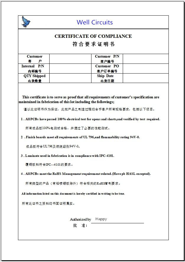
- CoC Report
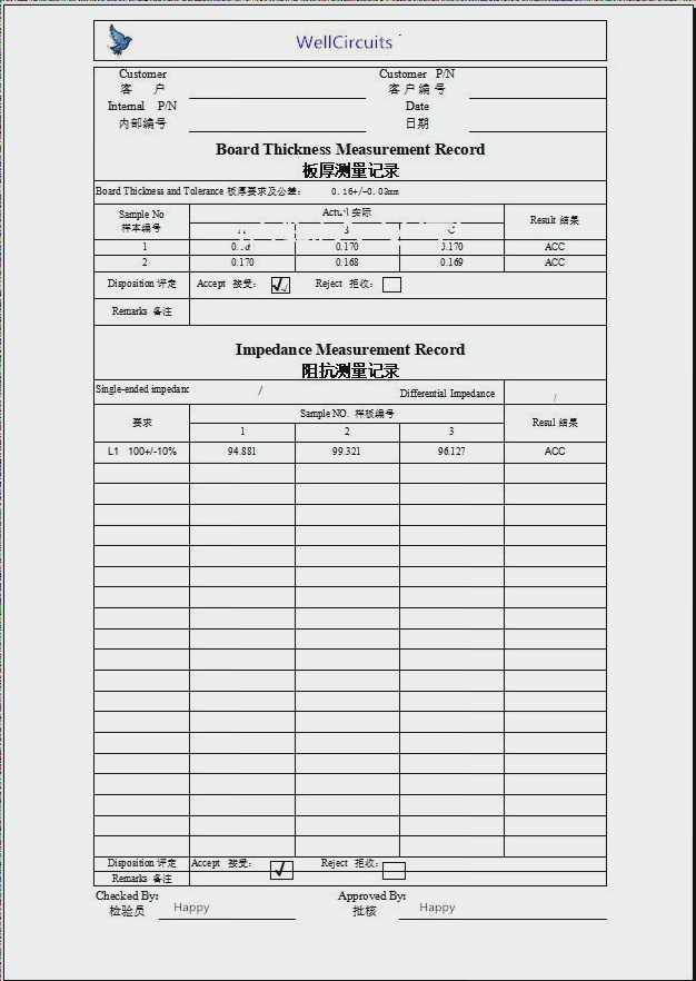
- Outgoing Report
- Impedance Mesurement
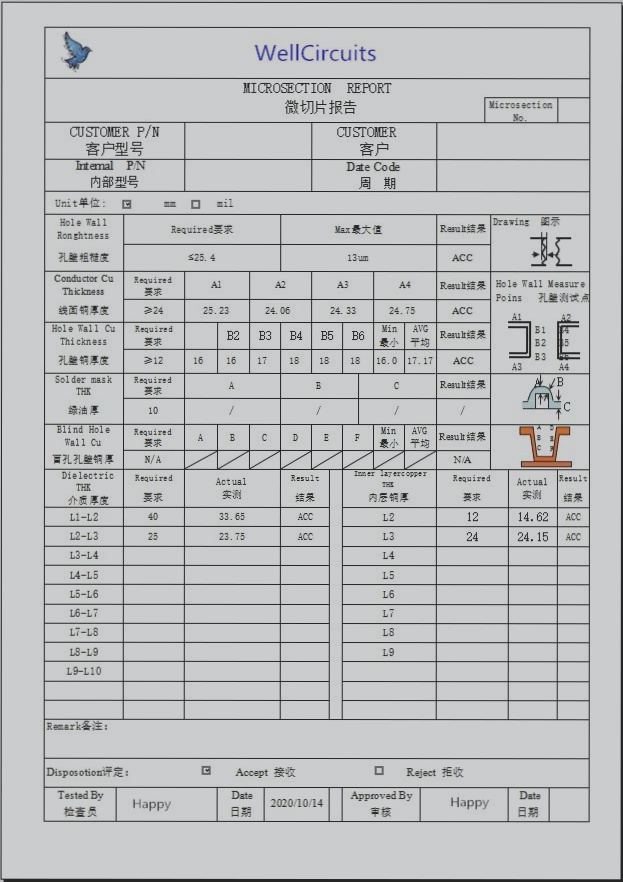
- Microsection Report
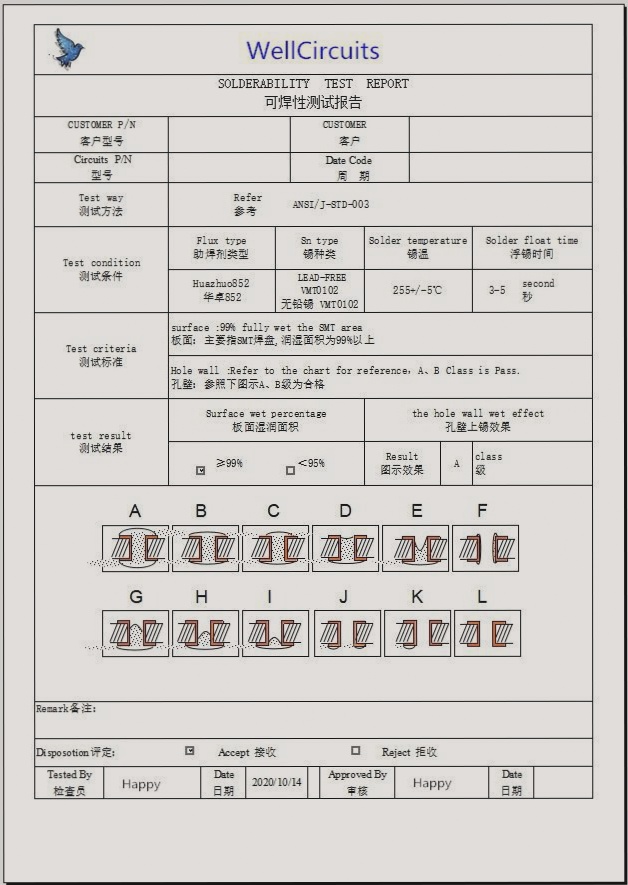
- Solderability Report
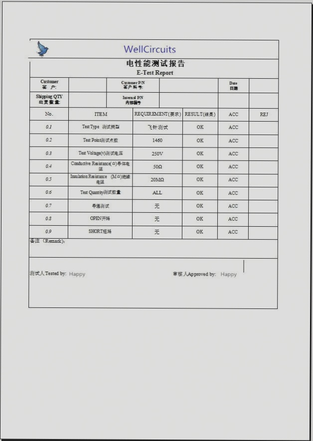
- E- test Report



Reviews
There are no reviews yet.