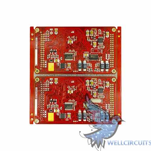
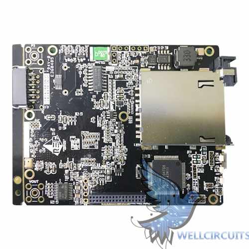
PCBA is the whole process of SMT mounting of PCB empty board and DIP plug-in.
SMT mounting mainly uses the mounting machine to mount some micro and small parts onto the PCB board.
DIP is “plug-in”, that is, insert parts on the PCB board. This is the form of plug-in integrated parts when some parts are large and not suitable for mounting technology.
Note: SMT and DIP are both ways to integrate parts on the PCB. The main difference is that SMT does not need to drill holes on the PCB, and DIP needs to insert the pin pin of the part into the drilled hole.
Summary: PCBA generally refers to a processing process, which can also be understood as a finished circuit board, that is, PCBA can only be counted after all the processes on the PCB are completed. The PCB of the circuit board factory refers to an empty printed circuit board with no parts on it. In general, PCBA is a finished board; The PCB is bare.
Get Instant Quote Now
WellCircuits ADVANTAGES
- In-house engineering
- Turnkey FPC & Assembly Solution
- Quick-turn up to 48hrs
- In-house assembly lines
- Support Prototype | Series Production


Reviews
There are no reviews yet.