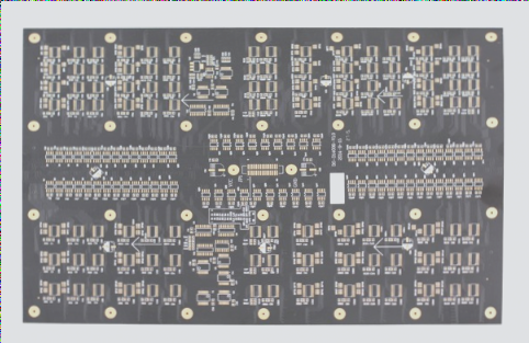
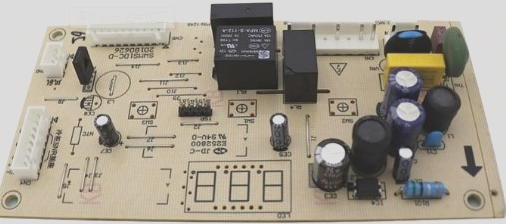
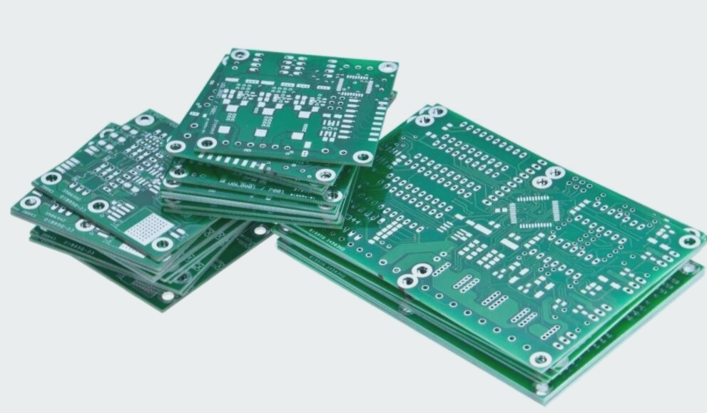
In the industry, a printed circuit board (PCB) with a copper foil thickness of 105 μm (≥3 oz) or greater is referred to as a thick copper printed circuit board. Recently, the application field and demand for thick copper PCBs have rapidly expanded, making them a favored variety with promising market development potential. The vast majority of thick copper printed circuit boards serve as high-current substrates, primarily utilized in two areas: power modules and automotive electronic components. The trend for these high-current substrates is to support larger currents, necessitating effective heat dissipation from bigger devices, which has led to an increase in copper foil thickness. For instance, the use of 210 μm thick copper foil for high-current substrates has become standard; additionally, the conductor layer thickness in substrates intended to replace traditional busbars and wiring harnesses in vehicles, robots, and power supplies has reached between 400 μm and 2000 μm.

105 μm thick copper printed circuit boards face challenges in solder mask production. The ink thickness on the substrate is limited (as navigation marks have specific requirements), and excessive ink thickness can lead to solder resist cracks post-welding of the PCB. Consequently, electrostatic spraying or spraying technology is not feasible. Currently, the industry relies solely on traditional screen printing: either applying multiple solder masks or fabricating the substrate first, filling it with solder mask, and treating it like a standard PCB for normal solder mask printing. However, screen printing often results in quality issues, including solder resist holes, broken bridges, and bubbles between lines. This research aims to explore how to enable electrostatic spraying or spraying processes while ensuring the solder mask thickness at the substrate position remains manageable.
1 Method Implementation
1.1 Planning Stage
(1) Direction Planning: The proposed method involves modifying the design engineering data to create solder mask exposure films. After multiple solder masks, the ink on the substrate is developed while retaining ink along the edges of the lines. The process is then treated as standard PCB production, ensuring only one solder mask is present on the substrate, avoiding circuit redness.
(2) Process Planning: The workflow includes pre-treatment of solder mask, hole plugging, electrostatic spraying, counter-exposure (using specially designed film), development, post-baking of the solder mask, pre-treatment, hole plugging, electrostatic spraying, normal negative counter-exposure, development, and final resist baking after welding.
2.2 Test Phase
(1) Initial Multiple Solder Mask Production: Utilize electrostatic spraying or spraying technology (ensuring no solder enters the holes) along with specially designed exposure film materials for the solder mask.
(2) Final Solder Mask Production: Again employ electrostatic spraying or spraying technology (with the same precautions) using standard solder mask exposure film materials.
(3) Measurement of Ink Thickness at the Substrate Position.
2.3 Standardized Promotion Stage
Using the data and processes developed from this design, small to medium batch production is tested, yielding consistent results with initial test phases. For all copper printed circuit boards thicker than 105 mm, this process significantly enhances product quality in solder mask production.
3 Results
The newly developed processes not only enable the effective use of electrostatic spraying or spraying for copper printed circuit boards thicker than 105 mm, overcoming limitations of traditional screen printing, but also prevent solder mask cracks due to excessive ink thickness at the substrate position. This allows for smooth mass production of solder masks while meeting customer quality standards. Following the implementation of this process, the bottleneck for mass production of copper printed circuit boards of 105 mm thickness or more has been resolved, reducing the scrap rate from 1.2% to 0.3%. Consequently, these PCBs are now reliable for applications in power products, communications, electric power, and aerospace.
—
Let me know if you need anything else!


