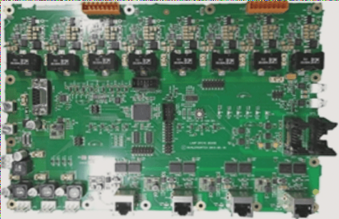
1. A printed circuit board (PCB) is found in nearly every electronic device. If an electronic component is present in a device, it is typically mounted on a PCB of varying sizes.

2. Besides securing the individual components, the primary role of a PCB is to provide electrical connections between these parts. As electronic devices become increasingly complex, the number of components required grows, leading to a denser arrangement of circuits and parts on the PCB.

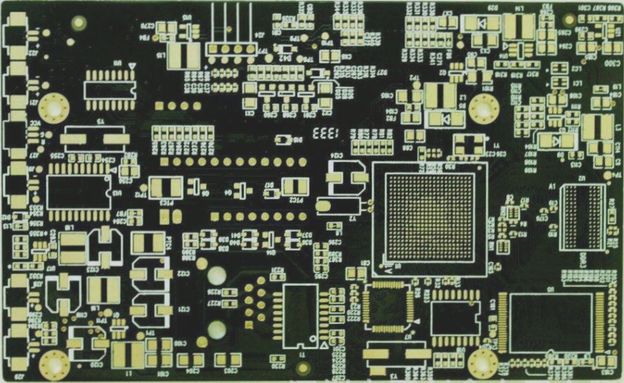
3. The standard PCB generally looks like this: the bare board, which has no components mounted, is commonly referred to as a “Printed Wiring Board” (PWB).

4. The base material of the board is typically made from insulating and heat-resistant materials that are also rigid and not easily bent. The thin circuit material visible on the surface is copper foil. Originally, the entire board was coated with copper foil, but a portion of it is etched away during the manufacturing process, leaving behind a network of small conductive paths.

5. These conductive paths are referred to as conductor patterns or traces, and their purpose is to provide the necessary electrical connections between the various components on the PCB.

1. If there are components on the PCB that need to be removed or reinstalled after production, a socket is used for component installation. Since the socket is directly soldered to the board, components can be easily assembled or disassembled as needed. Shown below is a ZIF (Zero Insertion Force) socket, which allows components (in this case, the CPU) to be inserted or removed with minimal effort. The locking mechanism next to the socket secures the component after insertion.

2. When connecting two PCBs, an edge connector, commonly referred to as a “golden finger,” is typically used. The golden finger has multiple exposed copper pads, which are actually part of the PCB’s routing. During connection, the golden finger of one PCB is inserted into the corresponding slot on the other PCB, commonly known as the expansion slot. In computers, display cards, sound cards, and other similar interface cards are connected to the motherboard via golden fingers.

3. The green or brown color seen on the PCB is the solder mask. This layer acts as an insulating protective barrier, safeguarding the copper traces and preventing incorrect component placement during soldering. A layer of silkscreen is printed over the solder mask, typically in white, displaying text and symbols to indicate the placement of components on the board. This printed layer is also known as the “legend.”

4. **Single-Sided Boards**

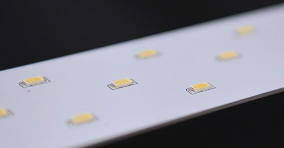
As previously mentioned, in the simplest type of PCB, components are placed on one side, and the routing is on the other. Since the traces are only on one side, this type of PCB is referred to as single-sided. Single-sided boards impose significant design limitations, as traces cannot overlap and must follow separate paths. As a result, single-sided boards were primarily used in early circuit designs.

5. **Double-Sided Boards**

A double-sided PCB has traces on both sides. To enable interconnection between these two sides, a proper circuit link is required, typically achieved through a via. A via is a small hole in the PCB that is plated with metal, allowing connections between traces on both sides. Because a double-sided board effectively doubles the available area compared to a single-sided board, and allows for more flexible routing (including trace paths that can be routed to the other side), it is more suitable for complex circuits.

6. **Multi-Layer Boards**

To increase routing capacity even further, multi-layer PCBs stack multiple single- or double-sided boards. An insulating layer is placed between each board and the layers are then bonded together. The number of layers in the PCB corresponds to the number of independent routing layers, with most boards featuring an even number of layers, including the two outermost layers. Typical motherboards have 4 to 8 layers, though technically, it is possible to manufacture PCBs with up to 100 layers. High-performance supercomputers often use heavily layered motherboards, though multi-layered designs have become less common in recent years, as clusters of regular computers can now perform similar tasks. Due to the tight integration of the layers, the actual number of layers is often not visible, but upon closer inspection of the motherboard, you might be able to identify it.

Leave a Comment

Contact

WellCircuits
More than PCB

Upload your GerberFile(7z,rar,zip)