Sure, here’s the revised text with some adjustments for clarity and grammar:
Packing: All PCBs must be packed in vacuum bags with moisture-proof beads inside. The outer packaging must not be damaged.
Text printing: The model, version, BOM, and ECN must be consistent. Text and model characters, logos, UL, FCC, CE, or lead-free marks must not have defects, typos, missing prints, unclear prints, or other issues.
Surface: The PCB surface must not have tin residue in the traces. Solder resist, glue traces, and incorrect labels are not allowed. Non-wire conductors such as copper residue must be at least 2.5mm away from traces. The area must be ≤0.25mm². Scratches should be less than 10mm in length and less than 0.2mm in width without damaging the substrate, with a maximum of two allowed. Non-tinned and gold-plated traces, as well as exposed copper areas, must not exceed 0.5mm². Green solder mask wrinkles should not exceed 25.4mm and must not peel off, ensuring no impact on solder paste screen printing.
Circuit: PCB traces and pads must not be warped or repaired. Scratch lengths should be less than 5mm with widths less than 0.2mm, and no more than two instances of exposed copper. Repairs are not allowed on gold finger or CHIP component pads.

Certainly! Here’s the revised and polished version of the text:
Flatness: The PCB board’s warpage shall not exceed 8/1000 of the diagonal of the board.
Lamination: No substrate delamination is permitted. There should be no cracks at the edges of the substrate or pad holes. Blistering must be ≥ 0.7mm away from the trace, with maximum blister diameter not exceeding 0.7mm, ensuring it remains within the component coverage area. Substrate edges should have ≤ 0.2mm uneven burrs or unevenness, with no exposed conductors on the board surface.
Pad: Trim edges should be smooth, clean, and shiny under normal conditions. Discoloration in solder joints or pads will result in rejection.
Size: Use card gauge to measure puzzle board size, verify BOM data, and promptly document each batch of incoming circuits or new PCB versions after changes.
Trimming and drilling: No porous, leaking, inconsistently sized, plugged, cracked, oxidized, or fouled holes that affect soldering are permitted.
Gold finger: The cutting edge must be smooth and free from stains such as green oil, tin, electroplating pores, bubbles, exposed copper, or nickel.
Oxidation: No obvious discoloration, redness, whitish/black stains, or unclean oil marks. Exposed copper scratches should not exceed 5mm per strip or two per side.
Key checks: Use a microscope to inspect for oxidation on areas like BGA pads and gold fingers.

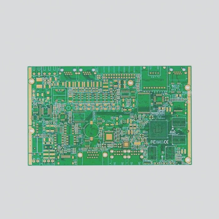
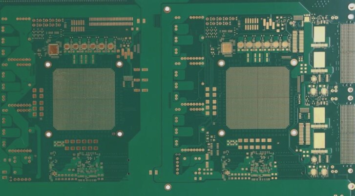
Multilayer PCB Inspection Standards for Professional PCB Manufacturers
The multilayer PCB consists of double-layer boards with highly precise circuit layouts and a diverse array of complex components. Ensuring these components meet specifications is crucial. Therefore, rigorous testing is essential before manufacturing and packaging multilayer PCBs to ensure both component quality and solderability. Typically, ICT (in-circuit testing) or automatic testing machines are employed, utilizing bed-of-nails fixtures to contact all measurement points on the board. What are the key considerations during this testing process?
1. The PCB’s zero soldering pads cannot serve as test points; instead, dedicated test pads should be designed. These pads should be situated on the same side of the multilayer PCB to reduce inspection costs.
2. To ensure secure connections and prolong probe lifespan, choose softer, easily penetrating, and non-oxidizing metals for the test probes.
3. Maintain a margin of approximately 5 mm around each test point on the multilayer PCB, and ensure a minimum distance of 1 mm between probes and components to prevent interference.
4. Ensure each test point has a diameter of no less than 0.4 mm, with adjacent test points spaced approximately 2.54 mm apart, but not less than 1.27 mm.
5. Distribute all test points evenly across the multilayer PCB to minimize probe-induced stress concentrations. Place test breakpoints in different areas of the power lines on the PCB to facilitate decoupling of power supplies or pinpointing of faults.
Packing: All PCBs must be packed in vacuum bags with moisture-proof beads inside. The outer packaging must not be damaged.
Text printing: The model, version, BOM, and ECN must be consistent. Text and model characters, logos, UL, FCC, CE, or lead-free marks must not have defects, typos, missing prints, unclear prints, or other issues.
Surface: The PCB surface must not have tin residue in the traces. Solder resist, glue traces, and incorrect labels are not allowed. Non-wire conductors such as copper residue must be at least 2.5mm away from traces. The area must be ≤0.25mm². Scratches should be less than 10mm in length and less than 0.2mm in width without damaging the substrate, with a maximum of two allowed. Non-tinned and gold-plated traces, as well as exposed copper areas, must not exceed 0.5mm². Green solder mask wrinkles should not exceed 25.4mm and must not peel off, ensuring no impact on solder paste screen printing.
Circuit: PCB traces and pads must not be warped or repaired. Scratch lengths should be less than 5mm with widths less than 0.2mm, and no more than two instances of exposed copper. Repairs are not allowed on gold finger or CHIP component pads.
Certainly! Here’s the revised and polished version of the text:
Flatness: The PCB board’s warpage shall not exceed 8/1000 of the diagonal of the board.
Lamination: No substrate delamination is permitted. There should be no cracks at the edges of the substrate or pad holes. Blistering must be ≥ 0.7mm away from the trace, with maximum blister diameter not exceeding 0.7mm, ensuring it remains within the component coverage area. Substrate edges should have ≤ 0.2mm uneven burrs or unevenness, with no exposed conductors on the board surface.
Pad: Trim edges should be smooth, clean, and shiny under normal conditions. Discoloration in solder joints or pads will result in rejection.
Size: Use card gauge to measure puzzle board size, verify BOM data, and promptly document each batch of incoming circuits or new PCB versions after changes.
Trimming and drilling: No porous, leaking, inconsistently sized, plugged, cracked, oxidized, or fouled holes that affect soldering are permitted.
Gold finger: The cutting edge must be smooth and free from stains such as green oil, tin, electroplating pores, bubbles, exposed copper, or nickel.
Oxidation: No obvious discoloration, redness, whitish/black stains, or unclean oil marks. Exposed copper scratches should not exceed 5mm per strip or two per side.
Key checks: Use a microscope to inspect for oxidation on areas like BGA pads and gold fingers.
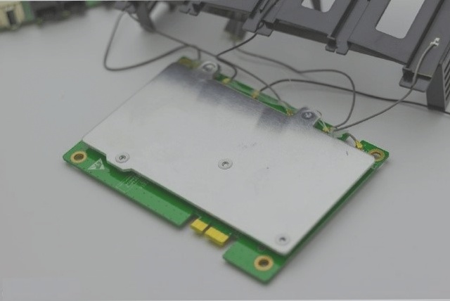
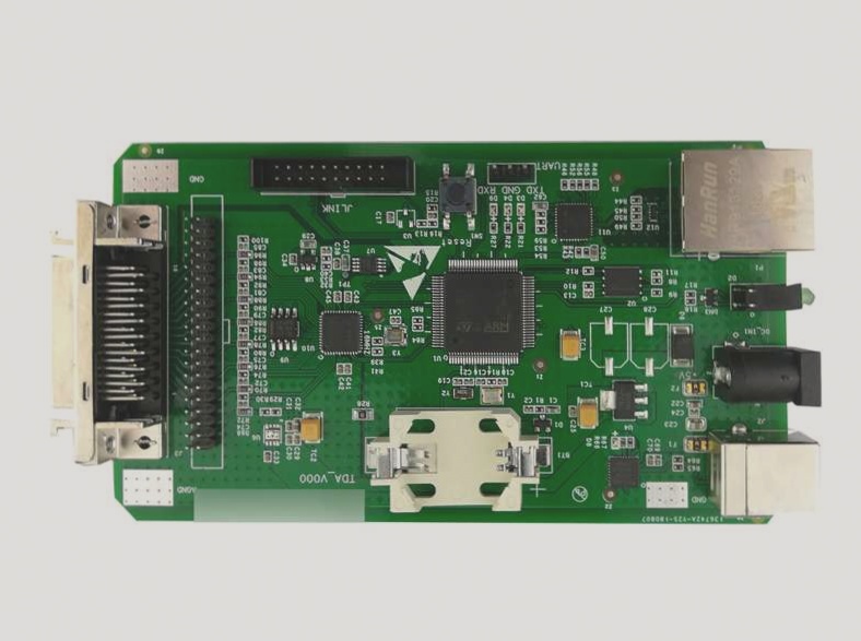
Multilayer PCB Inspection Standards for Professional PCB Manufacturers
The multilayer PCB consists of double-layer boards with highly precise circuit layouts and a diverse array of complex components. Ensuring these components meet specifications is crucial. Therefore, rigorous testing is essential before manufacturing and packaging multilayer PCBs to ensure both component quality and solderability. Typically, ICT (in-circuit testing) or automatic testing machines are employed, utilizing bed-of-nails fixtures to contact all measurement points on the board. What are the key considerations during this testing process?
1. The PCB’s zero soldering pads cannot serve as test points; instead, dedicated test pads should be designed. These pads should be situated on the same side of the multilayer PCB to reduce inspection costs.
2. To ensure secure connections and prolong probe lifespan, choose softer, easily penetrating, and non-oxidizing metals for the test probes.
3. Maintain a margin of approximately 5 mm around each test point on the multilayer PCB, and ensure a minimum distance of 1 mm between probes and components to prevent interference.
4. Ensure each test point has a diameter of no less than 0.4 mm, with adjacent test points spaced approximately 2.54 mm apart, but not less than 1.27 mm.
5. Distribute all test points evenly across the multilayer PCB to minimize probe-induced stress concentrations. Place test breakpoints in different areas of the power lines on the PCB to facilitate decoupling of power supplies or pinpointing of faults.
