Engaging in high-frequency PCB design requires not only solid foundational theoretical knowledge but also extensive practical experience in PCB production. This means that both the schematic design and the PCB layout must be approached with the high-frequency operating environment in mind, ensuring the design is optimized for performance and efficiency.
1. **PCB Layout Design**
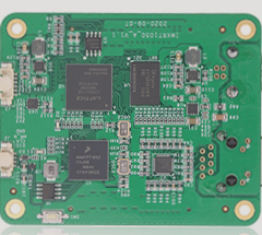
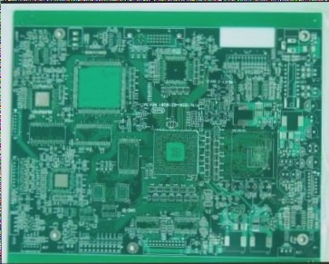
While Protel offers an automatic layout function, it does not fully meet the specific demands of high-frequency circuits. In practice, the layout process often relies on the designer’s expertise and is adjusted based on the particular requirements of the design. The positions of certain components are manually optimized and refined before being integrated with the automatic layout, allowing the overall PCB design to be completed. The effectiveness of the layout directly impacts the product’s lifespan, stability, EMC (electromagnetic compatibility), and other critical factors. Therefore, the design must take into account the overall layout of the circuit board, the routing feasibility, manufacturability, mechanical structure, heat dissipation, EMI (electromagnetic interference), reliability, and signal integrity, among other considerations.
Typically, components that are fixed due to mechanical constraints are placed first, followed by larger, special components, and finally smaller components. In addition, careful attention should be paid to the routing requirements; high-frequency components should be placed as close together as possible, and signal traces should be kept as short as feasible to minimize cross-interference between signal lines.

**1.1 Placement of Positioning Components Related to Mechanical Dimensions**
Power sockets, switches, PCB interconnects, indicator lights, and similar components are all considered positioning elements related to mechanical dimensions. Typically, the interface between the power supply and the PCB is placed at the PCB’s edge, with a recommended clearance of 3 mm to 5 mm from the edge. Light-emitting diodes should be placed precisely based on design requirements. Switches and fine-tuning components, such as adjustable inductors and resistors, should be positioned near the edge of the PCB for easier access and adjustment. Components that require frequent replacement should be located in areas with minimal component density to facilitate quick and easy replacement.
**1.2 Placement of Special Components**
High-power devices like tubes, transformers, and rectifiers generate significant heat during high-frequency operation. Therefore, ventilation and heat dissipation must be carefully considered in the layout, with these components positioned in areas where air circulation is optimal. High-power rectifiers and adjustment tubes should be equipped with heat sinks and kept away from transformers. Heat-sensitive components such as electrolytic capacitors should also be placed away from heat sources to avoid drying out the electrolyte, which could increase resistance, degrade performance, and impact circuit stability.
Components prone to failure, such as adjustment tubes, electrolytic capacitors, and relays, should be positioned with maintenance in mind. For test points that need frequent measurements, the layout should allow easy access to the test probes.
A 50 Hz leakage magnetic field is generated inside the power supply unit, which can interfere with low-frequency amplifiers when cross-coupled with them. Therefore, these components must be isolated or shielded. It is advisable to arrange each amplifier stage in a straight line according to the schematic. This arrangement ensures that the ground current for each stage is contained within that stage, preventing interference with other circuits. The input and output stages should be positioned as far apart as possible to minimize parasitic coupling.
To optimize signal transfer between circuit functional blocks, low-frequency circuits should be separated from high-frequency circuits, and analog circuits should be separated from digital circuits. Integrated circuits should be placed at the center of the PCB to facilitate connections with other devices.
Inductive components like inductors and transformers have strong magnetic coupling and should be placed orthogonally to one another to minimize interference. These components also generate significant magnetic fields, so they should be surrounded by adequate space or magnetic shielding to reduce their impact on nearby circuits.
High-frequency decoupling capacitors should be placed at strategic locations on the PCB. For example, an electrolytic capacitor (10 µF to 100 µF) should be positioned at the power input, while a 0.01 µF ceramic capacitor should be placed near the power pins of integrated circuits. Additionally, some circuits may require high- or low-frequency chokes to mitigate interference between circuits operating at different frequencies. This should be considered during schematic design, as improper planning could degrade circuit performance.
The spacing between components should be carefully considered, ensuring sufficient clearance to prevent breakdown or ignition between them.
For amplifiers incorporating push-pull or bridge circuits, particular attention should be paid to the symmetry of electrical parameters and the layout structure. This ensures that the distribution parameters of the symmetrical components are as consistent as possible.
Once the manual placement of main components is completed, a component locking method should be applied to prevent any movement during automatic layout. This can be done by executing the “Edit Change” command or selecting the “Locked” option in the component’s properties to prevent it from being moved during automatic routing.
**1.3 Placement of Common Components**
For standard components, such as resistors and capacitors, the layout should consider factors like the neat arrangement of components, the available space, ease of routing, and soldering convenience. The use of automated layout tools is recommended for these components.
PCB routing is a key aspect of high-frequency PCB design, based on a reasonable component layout. Routing includes both automatic and manual methods. Typically, key signal lines should be routed manually first, regardless of their number. After completing manual routing, a thorough inspection of these signal lines should be conducted. Once they pass inspection, the lines can be locked, and the remaining routing can be handled automatically. This approach combines manual and automatic routing to achieve optimal PCB layout.
If you have any PCB manufacturing needs, please do not hesitate to contact me.Contact me
1. **PCB Layout Design**
While Protel offers an automatic layout function, it does not fully meet the specific demands of high-frequency circuits. In practice, the layout process often relies on the designer’s expertise and is adjusted based on the particular requirements of the design. The positions of certain components are manually optimized and refined before being integrated with the automatic layout, allowing the overall PCB design to be completed. The effectiveness of the layout directly impacts the product’s lifespan, stability, EMC (electromagnetic compatibility), and other critical factors. Therefore, the design must take into account the overall layout of the circuit board, the routing feasibility, manufacturability, mechanical structure, heat dissipation, EMI (electromagnetic interference), reliability, and signal integrity, among other considerations.
Typically, components that are fixed due to mechanical constraints are placed first, followed by larger, special components, and finally smaller components. In addition, careful attention should be paid to the routing requirements; high-frequency components should be placed as close together as possible, and signal traces should be kept as short as feasible to minimize cross-interference between signal lines.

**1.1 Placement of Positioning Components Related to Mechanical Dimensions**
Power sockets, switches, PCB interconnects, indicator lights, and similar components are all considered positioning elements related to mechanical dimensions. Typically, the interface between the power supply and the PCB is placed at the PCB’s edge, with a recommended clearance of 3 mm to 5 mm from the edge. Light-emitting diodes should be placed precisely based on design requirements. Switches and fine-tuning components, such as adjustable inductors and resistors, should be positioned near the edge of the PCB for easier access and adjustment. Components that require frequent replacement should be located in areas with minimal component density to facilitate quick and easy replacement.
**1.2 Placement of Special Components**
High-power devices like tubes, transformers, and rectifiers generate significant heat during high-frequency operation. Therefore, ventilation and heat dissipation must be carefully considered in the layout, with these components positioned in areas where air circulation is optimal. High-power rectifiers and adjustment tubes should be equipped with heat sinks and kept away from transformers. Heat-sensitive components such as electrolytic capacitors should also be placed away from heat sources to avoid drying out the electrolyte, which could increase resistance, degrade performance, and impact circuit stability.
Components prone to failure, such as adjustment tubes, electrolytic capacitors, and relays, should be positioned with maintenance in mind. For test points that need frequent measurements, the layout should allow easy access to the test probes.
A 50 Hz leakage magnetic field is generated inside the power supply unit, which can interfere with low-frequency amplifiers when cross-coupled with them. Therefore, these components must be isolated or shielded. It is advisable to arrange each amplifier stage in a straight line according to the schematic. This arrangement ensures that the ground current for each stage is contained within that stage, preventing interference with other circuits. The input and output stages should be positioned as far apart as possible to minimize parasitic coupling.
To optimize signal transfer between circuit functional blocks, low-frequency circuits should be separated from high-frequency circuits, and analog circuits should be separated from digital circuits. Integrated circuits should be placed at the center of the PCB to facilitate connections with other devices.
Inductive components like inductors and transformers have strong magnetic coupling and should be placed orthogonally to one another to minimize interference. These components also generate significant magnetic fields, so they should be surrounded by adequate space or magnetic shielding to reduce their impact on nearby circuits.
High-frequency decoupling capacitors should be placed at strategic locations on the PCB. For example, an electrolytic capacitor (10 µF to 100 µF) should be positioned at the power input, while a 0.01 µF ceramic capacitor should be placed near the power pins of integrated circuits. Additionally, some circuits may require high- or low-frequency chokes to mitigate interference between circuits operating at different frequencies. This should be considered during schematic design, as improper planning could degrade circuit performance.
The spacing between components should be carefully considered, ensuring sufficient clearance to prevent breakdown or ignition between them.
For amplifiers incorporating push-pull or bridge circuits, particular attention should be paid to the symmetry of electrical parameters and the layout structure. This ensures that the distribution parameters of the symmetrical components are as consistent as possible.
Once the manual placement of main components is completed, a component locking method should be applied to prevent any movement during automatic layout. This can be done by executing the “Edit Change” command or selecting the “Locked” option in the component’s properties to prevent it from being moved during automatic routing.
**1.3 Placement of Common Components**
For standard components, such as resistors and capacitors, the layout should consider factors like the neat arrangement of components, the available space, ease of routing, and soldering convenience. The use of automated layout tools is recommended for these components.
PCB routing is a key aspect of high-frequency PCB design, based on a reasonable component layout. Routing includes both automatic and manual methods. Typically, key signal lines should be routed manually first, regardless of their number. After completing manual routing, a thorough inspection of these signal lines should be conducted. Once they pass inspection, the lines can be locked, and the remaining routing can be handled automatically. This approach combines manual and automatic routing to achieve optimal PCB layout.
If you have any PCB manufacturing needs, please do not hesitate to contact me.Contact me


