
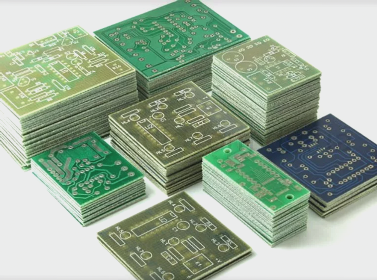
PROTEL99SE PCB Design Technology
Software Environment Setup
- 1. Safety Distance Setting:
- 2. Wiring Layer and Direction Setting:
- 3. Via Options Setting:
- 4. Line Width Option Setting:
- 5. Copper Coating Connection Option Setting:
- 6. Physical Aperture Setting:
The Clearance Constraint item in PROTEL99SE software specifies the distance between routing, pads, vias, etc. of different networks on the board. For single or double panels, the preferred value is 10-12mil; for PCBs with four or more layers, it is 6-8mil.
Routing Layers in PROTEL99SE software determine the routing layer and direction for each layer. Default values are generally used.
Routing Via Style specifies the minimum, maximum, and preferred values of via inner and outer diameters. Settings vary based on the number of layers in the PCB.
Width Constraint of Routing specifies the wiring width. Different settings apply to single/double panels and PCBs with four or more layers. Special settings can be applied for specific networks.
The Polygon Connect Style in PROTEL99SE software defines the copper coating connection method. Specific attributes such as Relief Connect mode, Conductor Width, Conductors, and Angle need to be set.
Hole Size Constraint item specifies the size of physical apertures like positioning and installation holes. Default values can be used for other items.
PROTEL99SE PCB Software Parameter Setting
- 1. Visual Grid Option Setting:
- 2. Capture and Device Moving Grid Option Setting:
From Design Options Layer, select various options like Top solver, Top overlay, Keepout, and Multi Layer. Set the Visible Grid size to 10mil (upper) and 100mil (lower).
In Design Options, set the capture and device moving grid sizes to 10mil. Specify the Electrical Grid range, Visible Kind, and Measurement Unit.
DRC Verification Settings
- 1. Tools Design Rules Check:
- 2. Add Device Library
Set options for Clear Constraints, Max/Min Width Constraints, Short Circuit Constraints, Unrouted Net Constraints, Max/Min Hole Size, and more based on design requirements.

PCB Design Process
- Component Selection
- Importing Network Table
- Layout of Components
- PCB Wiring
- Placement of Silk Screen and Chinese Characters
- Large Area Paving
Component Selection
When designing a PCB, it is crucial to select components from the corresponding library based on the schematic diagram.
Importing Network Table
Ensure error-free import of the network table before proceeding with the design. PCB size, positioning hole location, and component placement are key considerations.
Layout of Components
Follow the principle of beautiful and orderly layout, ensuring proper density and symmetry between main components and modules. Check for consistency in board size, component conflicts, and thermal management.
PCB Wiring
Use automatic routing with manual adjustments for efficient wiring. Prioritize ground wire, power line, and clock line routing. Consider aesthetics and electrical characteristics during the routing process.
Placement of Silk Screen and Chinese Characters
Strategically place product names, model numbers, logos, and Chinese characters for clear identification. Pay attention to font placement and avoid routing over critical markings.
Large Area Paving
Utilize Polygon Plane for large area coverage, connecting to GND, and setting appropriate grid size and track width for efficient PCB design.
Important Steps for PCB Design
- Before starting large-area paving, ensure the safety clearance value is set to 25mil.
- After completing large-area paving, remember to restore the safety clearance value.
- Use the FILL filling layer in areas where wiring is not desired, such as near specific components like crystal oscillators and voltage regulators.
- Consider adding teardrops to improve connection reliability, but be mindful that they may affect the aesthetics of the board.
- Perform a thorough Design Rules Check (DRC) to identify and correct any errors.
- During PCB production, ensure components’ names and packages are removed to protect technical information.
When creating PCBs, attention to detail is crucial, especially when it comes to wiring accuracy. Following proper design rules and procedures is essential to ensure a successful outcome.
For RF PCBs, specific considerations like thickness and material type play a significant role in the manufacturing process. It is recommended to follow industry standards for RF PCB fabrication.
 العربية
 简体中文
简体中文 Nederlands
 English
 Français
 Deutsch
 Italiano
 日本語
日本語 한국어
한국어 Português
 Русский
 Español
 ไทย
ไทย