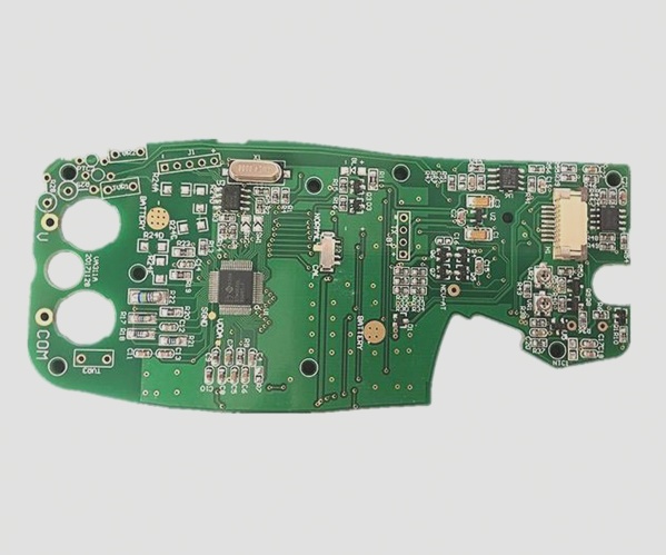
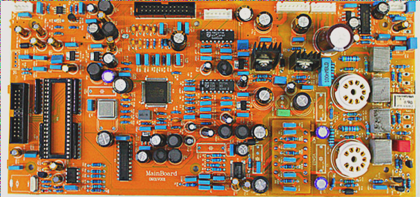
The PCBA processing is currently a highly developed method, primarily utilized for the assembly of electronic devices with a significant degree of integration. However, it is essential to conduct a pre-production meeting during the PCB processing phase. Additionally, the procurement and inspection of electronic components provided by the PCB must take place, along with the establishment of a dedicated PCB input inspection station to rigorously check specific items, ensuring that components are free of defects. Only through these measures can we guarantee quality and minimize extensive rework and repairs. I will now detail the relevant content.
PCBA processing
1. How to control the quality of PCBA processing
1. Holding a pre-production meeting after receiving the PCBA order is crucial. This process involves analyzing the PCB Gerber files and submitting manufacturability reports (DFM) tailored to various customer requirements. Many smaller manufacturers often overlook this step, leading to potential quality issues stemming from inadequate PCB design and resulting in excessive rework and repair efforts.

2. Purchase and Inspection of Electronic Components Provided by PCBA
The procurement channels for electronic components must be rigorously controlled, ensuring that products are sourced from reputable distributors and original manufacturers to avoid second-hand or counterfeit materials. Additionally, a dedicated PCBA incoming inspection station should be established to meticulously check the following items, ensuring all components are defect-free.
PCB: Verify the temperature test of the reflow oven, ensure that through holes without flying leads are neither blocked nor leaking, and check for any warping on the board’s surface.
IC: Confirm that the screen printing matches the BOM precisely and maintain storage under consistent temperature and humidity conditions.
3. SMT Assembly
Solder paste printing and reflow oven temperature control are critical aspects of assembly, necessitating high-quality laser templates with stringent processing requirements. Depending on the PCB specifications, adjustments may be needed for the steel mesh or U-shaped holes, aligning with process demands. Proper temperature control of the reflow oven is essential for solder paste wetting and mesh adhesion, following standard SOP guidelines. Furthermore, strict adherence to AOI testing can significantly minimize defects arising from human error.
4. Plug-In Processing
In the plug-in stage, the mold design for wave soldering is pivotal. PE engineers should continuously refine their techniques and insights on mold usage to enhance productivity dramatically.
5. PCB Processing Board Testing
For orders requiring PCBA testing, key evaluations include ICT (In-Circuit Testing), FCT (Functional Testing), combustion tests (aging tests), temperature and humidity tests, and drop tests.
**Precautions in PCBA Processing**
1. The minimum distance between copper foil and the board edge is 0.5mm, with a minimum distance of 5.0mm between components and the board edge, and 4.0mm between pads and the board edge.
2. The minimum gap between copper foils is 0.3mm for single-sided boards and 0.2mm for double-sided boards. (When designing double panels, ensure that metal shell components contact the PCB during insertion. The top pad should not be exposed and must be covered with silk screen oil or solder mask.)
3. Jumpers must not be placed beneath ICs or large-volume metal components like potentiometers and motors.
4. Electrolytic capacitors must not touch heating components such as transformers, thermistors, high-power resistors, or radiators. The minimum distance between radiators and electrolytic capacitors is 10mm, while other components must maintain a distance of 2.0mm from the radiator.
5. Larger components (e.g., transformers, electrolytic capacitors with a diameter of 15mm or more, and high-current sockets) require enlarged pads.
6. Minimum line widths are 0.3mm for single panels and 0.2mm for double panels (the minimum copper foil width on the side must also be 1.0mm).
7. No copper foil (except for grounding) or components should be present within a 5mm radius of the screw hole, unless specified by the structural drawing.
8. The pad size (diameter) for general through-hole mounting components should be twice the aperture, with a minimum of 1.5mm for double-sided boards and 2.0mm for single-sided boards. (If round pads are not feasible, alternative shapes can be used.)
The above highlights the precautions related to quality control and the processing procedures of PCBA manufacturing.
PCBA processing
1. How to control the quality of PCBA processing
1. Holding a pre-production meeting after receiving the PCBA order is crucial. This process involves analyzing the PCB Gerber files and submitting manufacturability reports (DFM) tailored to various customer requirements. Many smaller manufacturers often overlook this step, leading to potential quality issues stemming from inadequate PCB design and resulting in excessive rework and repair efforts.

2. Purchase and Inspection of Electronic Components Provided by PCBA
The procurement channels for electronic components must be rigorously controlled, ensuring that products are sourced from reputable distributors and original manufacturers to avoid second-hand or counterfeit materials. Additionally, a dedicated PCBA incoming inspection station should be established to meticulously check the following items, ensuring all components are defect-free.
PCB: Verify the temperature test of the reflow oven, ensure that through holes without flying leads are neither blocked nor leaking, and check for any warping on the board’s surface.
IC: Confirm that the screen printing matches the BOM precisely and maintain storage under consistent temperature and humidity conditions.
3. SMT Assembly
Solder paste printing and reflow oven temperature control are critical aspects of assembly, necessitating high-quality laser templates with stringent processing requirements. Depending on the PCB specifications, adjustments may be needed for the steel mesh or U-shaped holes, aligning with process demands. Proper temperature control of the reflow oven is essential for solder paste wetting and mesh adhesion, following standard SOP guidelines. Furthermore, strict adherence to AOI testing can significantly minimize defects arising from human error.
4. Plug-In Processing
In the plug-in stage, the mold design for wave soldering is pivotal. PE engineers should continuously refine their techniques and insights on mold usage to enhance productivity dramatically.
5. PCB Processing Board Testing
For orders requiring PCBA testing, key evaluations include ICT (In-Circuit Testing), FCT (Functional Testing), combustion tests (aging tests), temperature and humidity tests, and drop tests.
**Precautions in PCBA Processing**
1. The minimum distance between copper foil and the board edge is 0.5mm, with a minimum distance of 5.0mm between components and the board edge, and 4.0mm between pads and the board edge.
2. The minimum gap between copper foils is 0.3mm for single-sided boards and 0.2mm for double-sided boards. (When designing double panels, ensure that metal shell components contact the PCB during insertion. The top pad should not be exposed and must be covered with silk screen oil or solder mask.)
3. Jumpers must not be placed beneath ICs or large-volume metal components like potentiometers and motors.
4. Electrolytic capacitors must not touch heating components such as transformers, thermistors, high-power resistors, or radiators. The minimum distance between radiators and electrolytic capacitors is 10mm, while other components must maintain a distance of 2.0mm from the radiator.
5. Larger components (e.g., transformers, electrolytic capacitors with a diameter of 15mm or more, and high-current sockets) require enlarged pads.
6. Minimum line widths are 0.3mm for single panels and 0.2mm for double panels (the minimum copper foil width on the side must also be 1.0mm).
7. No copper foil (except for grounding) or components should be present within a 5mm radius of the screw hole, unless specified by the structural drawing.
8. The pad size (diameter) for general through-hole mounting components should be twice the aperture, with a minimum of 1.5mm for double-sided boards and 2.0mm for single-sided boards. (If round pads are not feasible, alternative shapes can be used.)
The above highlights the precautions related to quality control and the processing procedures of PCBA manufacturing.


