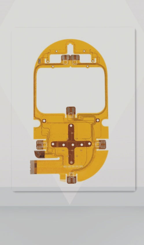
FR4 PCB Quality Inspection Techniques
X-ray Testing
- X-ray inspection post-assembly is crucial for detecting hidden solder joint defects in BGA, including short circuits, open circuits, insufficient solder, excessive solder, ball drop, and more.
Scanning Ultrasound Microscope (SAM)
- SAM can scan assembled circuit boards to detect hidden issues, with C-SAM plane scanning being the most common method.
Side View Method
- Optical amplification for side visual inspection, especially for examining small objects in restricted areas like BGA’s ball foot welding.
Screwdriver Strength Measurement
- Using torsion from a screwdriver to test solder joint strength, effective for identifying defects like floating solder joints or weld body cracking.
Microsection Method
- Requires sample cutting and preparation facilities to analyze solder joint issues in a destructive manner.
Infiltration Dyeing Method
- Immersing samples in a red dye solution to identify cracks and holes in solder joints, providing insights into joint completeness.
Hollow Ball Foot and Solder Joint Voids
Causes of Solder Joint Voids
- Various factors contribute to voids in solder joints, especially in BGA/CSP ball pin joints, worsened by high-heat lead-free soldering.
Organic Materials
- Flux in solder paste plays a significant role in void formation, with lower gas generation rate fluxes recommended to minimize voids.
Solder
- Surface tension of solder affects cohesion and cavity formation, with lower melting point solder balls prone to accumulating voids.
Surface Treatment
- Surface treatment films can impact hole formation, with silver immersion and OSP thickness affecting cavity formation.
Welding Pads and Micro-blind Holes
- Large welding pads and micro-blind holes are susceptible to cavities, strategies like adding outgoing ditches or electroplating copper can help reduce voids.
Hole Acceptance Specification
Factors Affecting Solder Joint Reliability in PCB Fabrication
Excessive holes in the ball foot can impact conductivity and heat transfer, leading to poor solder joint reliability. It is crucial to consider the upper limit of allowable hole diameter in the top section, which should not exceed 25% of the total contact area with a diameter of approximately 6%. Voids at the interface between the ball foot and the carrier plate or upper and lower welding pads of the FR4 PCB are a common cause of cracking.
Cavity Classification
BGA holes are classified into five types based on their location and source, although this classification may require future updates.
Bridging and Short Circuits
Bridging and short circuits between ball pins can occur due to various factors such as poor solder paste printing, incorrect component placement, manual adjustments post-placement, or tin splashing during fusion welding. Open circuits may result from issues like inadequate solder paste printing, post-placement adjustments, poor coplanarity, or inadequate soldering of the solder pad on the board.
Cold Solder and IMC Formation
Cold solder is a consequence of insufficient heat during the soldering process, leading to a lack of Intermetallic Compound (IMC) formation between the solder and the surface to be welded. Detailed examination using an optical microscope and microsection is essential to detect this issue accurately.

