The Process of PCB Duplication: Key Steps and Techniques
PCB duplication involves following several technical steps in order to replicate an original circuit board precisely. These include scanning it, creating a bill of materials and fabricating and assembling components of the new PCB board. Here is more detail:
1. Documenting the Original PCB
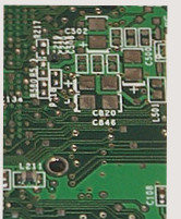
- Document your model, parameters and component positions using digital photography.
- Secure key part locations by taking digital pictures using your camera phone or digital imaging scanner.
2. Scanning and Cleaning
- Remove components and desolder remaining solder.
- Clean the PCB and scan it at a high resolution.
- Polish the layers until the copper shines.
3. Image Processing and Conversion
- Adjust contrast and brightness for clear distinction.
- Convert the image to black and white and save as BMP files.
4. Protel Format Conversion
- Convert BMP files to Protel format and align layers accurately.
5. Component Positioning
- Convert BMP to PCB format and position components.
- Repeat for all layers and delete unnecessary layers.
6. Layer Integration
- Combine top and bottom layers into a single image in Protel.
7. Printing and Verification
- Print layers onto transparent film at a 1:1 ratio.
- Overlay film on PCB to check alignment.
By following these steps meticulously, you can create a replica of the original PCB. Testing the electronic performance ensures the successful duplication of the board.
Note: Copying multilayer boards requires additional steps and precision due to their complexity. Extreme caution is advised, especially with internal vias and non-vias.
QuickPCB 2005 Double-Sided Board Copy Method:
- Scan and save top and bottom layers as BMP images.
- Use QuickPCB 2005 software to redraw the board and generate a B2P file.
- Repeat the process for the other layer to complete the duplication.
Quickpcb 2005 Multi-Layer Board Copy Method:
Copying a four-layer board involves duplicating two double-sided boards; for six layers or higher, it requires duplicating three double-sided boards. Multilayer boards present unique challenges due to hidden internal wiring; in order to reveal this interior wiring more fully on precision multilayer boards, move from layer by layer in your copying process.
Experience has shown that sandpaper polishing provides the most precise means of layering. Potion corrosion and tool stripping methods could potentially split layers apart and result in data loss; alternative methods, like potion corrosion or tool stripping, may lead to data being mislaid altogether.
After duplicating both top and bottom layers of a PCB, sandpaper can be used to polish its outermost surface layer and expose the inner layers. Regular hardware store sandpaper provides uniform grinding by exerting consistent pressure; using smaller sheets ensures a more precise grinding action.
Silk screen and green coating should usually be removed while copper traces and pads require special consideration. Polishing may take just minutes on a Bluetooth board, while for memory sticks it could take upwards of 10 minutes depending on their complexity and the effort needed to polish.
Grinding is currently the most widely adopted and cost-effective layering solution available, so experimentation using an old PCB board should be recommended as practice is highly encouraged. While grinding poses few technical difficulties, its repetitive nature could present additional technical obstacles.
WellCircuits supports quick turn PCB manufacturing. IF you have quick-turn PCB or PCBA RFQ, please feel free to contact info@wellcircuits.com.