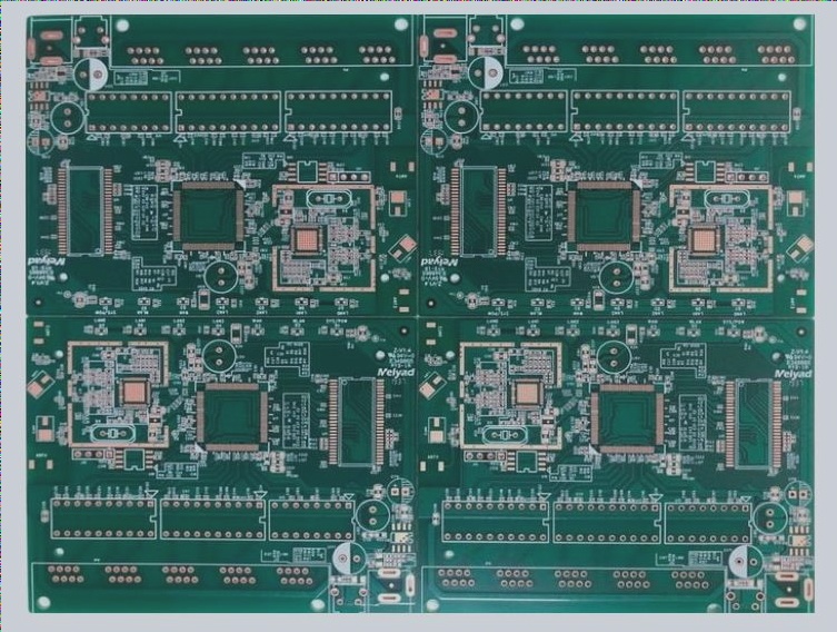
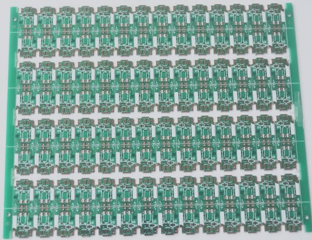
1. By utilizing low-cost PCBs (printed circuit boards), you can swiftly create a board in a few hours using almost any CAD plan, including free options. You can have your model board on your desk in just two days.
2. The layout rules in many software packages are excellent, and many vendors can manufacture PCBs with line widths and spacing down to 0.006 inches. This precision is suitable for low-frequency circuits, but RF circuits typically require 50Ω traces for correct operation.
3. As parts become smaller, the laws of physics remain unchanged. Therefore, a mini strip trace on a standard prototype board, which was 0.062 inches thick and measured 0.11 inches wide three decades ago, remains 0.11 inches wide today. While many surface-mount parts are much smaller than their predecessors, low-cost, two-layer prototype boards for RF prototyping may seem unsuitable for today’s small SMT (surface-mount technology) components.
4. To address this challenge, you can utilize a CPWG (coplanar waveguide over ground) structure to develop 50Ω RF traces on PCBs. A CPWG structure allows you to make the required trace width smaller than that of a microstrip structure.
5. Adding a copper ground plane on the top of the board, closer to a microstrip trace, introduces capacitance to the microstrip structure. To maintain the entire structure at 50Ω, you need to make the center trace more inductive by reducing its size—up to a certain point.
6. However, many online CPWG calculators fail when the ground-plane gap becomes less than approximately 30 to 50% of the trace width because the height of the copper traces on the board becomes a significant factor, contributing more capacitance than the calculators assume. As a result, the lines designed by these calculators often have excessive capacitance, reducing their impedance to less than 50Ω.
7. The equations used in several calculators become unreliable because modern PCBs differ physically from ICs. The most accurate way to design a CPWG on a PCB with a narrow gap-to-center trace ratio is to use a full 3-D electromagnetic simulator. This approach provides values for a few common structures.
8. Adhering to a minimal trace-to-trace spacing of 6 mils, I substituted, constructed, and tested a CPWG structure. For a standard 0.062-inch-thick FR-4 PCB material, a trace width of 0.032 inches with a gap of 0.006 inches is as close to 50Ω as achievable. It offers better than 40 dB return loss on the trace at 6 GHz.
9. This approach is superior to using a 0.11-inch-wide trace and is compatible with SMT-sized components. A 0603-sized SMT component and a common SMA (surface-mount assembly) edge-launch connector fit the line perfectly. Figure 1 illustrates several typical RF components on the fabricated PCB.
10. For components with larger pad dimensions than the 0.032-inch trace width, simply increase the spacing to the top ground plane to compensate. For instance, increase the spacing to the top plane of an 0805 SMT pad to about 0.008 inches and increase the top-plane spacing for a 1206 SMT-component pad to 0.012 inches to prevent excessive capacitance.
11. Figure 1: A nominally small SMT component fits well onto the 0.032-inch-wide CPWG 50Ω line structure. The 0603 resistors and capacitors, along with a small gallium-arsenide FET-amplifier SC-70 IC, also fit well. Adhering to common design guidelines, I pulled back the copper planes on the tested PCBs by 0.01 inches from the board edge. This pull-back, along with the edge-launch adapter, adds a slight amount of inductance to the transition. Cutting the pin to about half its original length yields approximately equal capacitance to balance the transition inductance.
12. The CPWG structure necessitates a solid ground plane under the trace; leaving cutouts in the bottom ground plane under the topside trace adds significant inductance to the structure, compromising high-frequency performance. Additionally, you need to “stitch” the top ground plane to the bottom ground plane with vias.
13. Place the stitching vias less than one-eighth of a wavelength of the highest frequency your circuit will use. Note that 0.1-inch spacing works well at frequencies higher than 10 GHz. The spacing of the stitching vias to the center trace follows the same rules.
14. You can easily incorporate enough vias in and around the trace to ensure proper functionality. Insufficient vias will result in a slight but rapid 0.5- to 1-dB drop in the S21 transmission characteristics instead of a linear loss slope with frequency. This effect can be observed using a VNA (vector network analyzer). Measuring the test board shows approximately 0.25 dB/in. of loss at 3 GHz and 1 dB/in. of loss at 10 GHz, including two edge-launch connectors.
15. To interface with an SMT component or an IC with narrower pads than 0.032 inches, limit the center conductor as close to the part as possible. If the suspension is physically small, it will have little effect until very high frequencies.