Offset Analysis and Improvement in PCB Daughter Board Design
1. Offset Analysis of PCB Daughter Board
When assembling a PCB daughter board, two stacking methods are commonly used. One involves securing the daughter board to the edge of the motherboard with rivets to minimize alignment concerns. The focus here is on the alignment in a stacking method where the daughter board is positioned centrally on the motherboard without pre-fixing with rivets.
The traditional approach involves adjusting the daughter board’s size and slot on the motherboard to ensure a snug fit and minimize gaps. However, matching a daughter board of similar size to the motherboard slot often leads to excessive offset issues rather than size compensation problems.
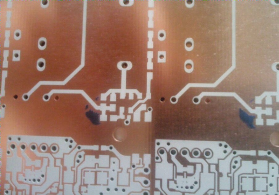
To address this, a gap of 0.15mm is typically set between the daughter board and motherboard to prevent significant deviation during assembly and ensure proper adhesive filling. In practice, measurements often reveal offsets larger than the intended 0.05mm, indicating a 0.1mm offset on certain sides of the daughter boards.
Excessive offsets not only impact conduction between layers but also affect bonding force due to insufficient glue in tight spaces. Improvements are needed in the bonding method of the daughter-mother board without clear positioning.

2. PCB Offset Improvement
PCB manufacturers have introduced concave and convex grooves along the board edge to enhance positioning accuracy between mother and daughter boards. While this design improves alignment, it still faces challenges with inadequate glue filling at corners, leading to risks of delamination and bursting.
Refinement in corner positioning is necessary to address the issue of insufficient glue filling at corners. New designs focusing on reducing the area of inadequate glue filling at corners can help minimize the risk of delamination and bursting. By incorporating rounded corners in the daughter-mother board design, glue flow is improved, ensuring complete corner filling and preventing significant corner misalignment.
Experiments involving the placement of a 0.2mm PCB pad at corresponding positions and drilling 0.2mm through holes have shown that daughter-mother board offsets can be controlled within 2 mils. Corner fillet widths of approximately 3 mils ensure thorough cross-sectional filling.