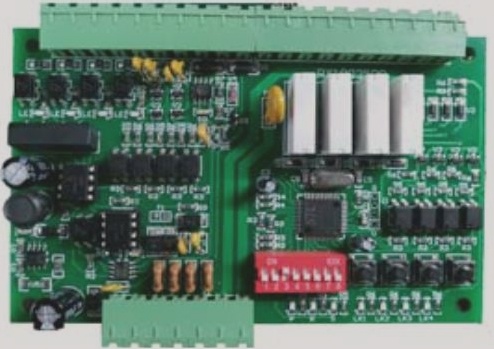
1. PCB Layout and Assembly
The initial step in PCB design involves crafting a circuit diagram. Once this diagram is finalized, the PCB design and layout phase commences. While circuit designs are typically represented on paper or in design software for clarity, such formalities aren’t strictly necessary for PCB design.
Although the connections in the circuit diagram and PCB layout remain consistent, the PCB layout is more advanced, specifically engineered to optimize space and adhere to various guidelines.
Numerous software options are available to assist in PCB design and layout. Programs like ADS or ARES can automatically generate the PCB layout from the circuit diagram; however, for more intricate designs, manual adjustments are often required to achieve optimal results. Connections can be routed either manually or through the capabilities of the PCB layout software.

1. They can be executed manually.
There are numerous types of PCB layouts. The layout for high-frequency RF PCBs differs from that of traditional digital applications.
To broadly categorize, we have digital PCB layouts, RF PCB layouts, antenna layouts, and power supply layouts. Each type has specific guidelines; for instance, in RF design, it’s crucial to minimize reflections on transmission lines and ensure that transmission lines do not come too close to one another, which could disrupt the signal.
Conversely, in digital application PCB layouts, we aim to keep copper tracks as close together as possible to conserve space and reduce costs. In antenna layouts, maximizing the design space is essential, while power supply layouts must prioritize effective heat dissipation.
2. PCBA processing and SMT assembly
Once the layout and design are finalized, the PCB assembly process commences. PCBs can be fabricated using various materials, with FR4 being the most common.
Different assembly methods, such as surface mount technology (SMT) or through-hole techniques, are employed to mount electronic components onto the PCB. It’s vital that the components selected are compatible with the chosen assembly process.
The decision regarding PCBA depends on the complexity of the PCB design. SMT is gaining popularity as it facilitates miniaturization of PCBs. For high-frequency RF PCBs, surface mount components help in reducing noise and reflections. For PCBs without such constraints, we opt for components that help minimize costs.
Layout costs are heavily influenced by the complexity of the design; multi-layer high-speed designs incur significantly higher costs. These costs encompass the tools needed for layout as well as the hiring of skilled designers. The cost of assembly is determined by the type and quality of the assembly process employed. Layout and design costs are interdependent.
Moreover, a poorly executed layout can lead to increased assembly costs, while a well-optimized PCB layout can effectively reduce both assembly and production expenses.
The initial step in PCB design involves crafting a circuit diagram. Once this diagram is finalized, the PCB design and layout phase commences. While circuit designs are typically represented on paper or in design software for clarity, such formalities aren’t strictly necessary for PCB design.
Although the connections in the circuit diagram and PCB layout remain consistent, the PCB layout is more advanced, specifically engineered to optimize space and adhere to various guidelines.
Numerous software options are available to assist in PCB design and layout. Programs like ADS or ARES can automatically generate the PCB layout from the circuit diagram; however, for more intricate designs, manual adjustments are often required to achieve optimal results. Connections can be routed either manually or through the capabilities of the PCB layout software.

1. They can be executed manually.
There are numerous types of PCB layouts. The layout for high-frequency RF PCBs differs from that of traditional digital applications.
To broadly categorize, we have digital PCB layouts, RF PCB layouts, antenna layouts, and power supply layouts. Each type has specific guidelines; for instance, in RF design, it’s crucial to minimize reflections on transmission lines and ensure that transmission lines do not come too close to one another, which could disrupt the signal.
Conversely, in digital application PCB layouts, we aim to keep copper tracks as close together as possible to conserve space and reduce costs. In antenna layouts, maximizing the design space is essential, while power supply layouts must prioritize effective heat dissipation.
2. PCBA processing and SMT assembly
Once the layout and design are finalized, the PCB assembly process commences. PCBs can be fabricated using various materials, with FR4 being the most common.
Different assembly methods, such as surface mount technology (SMT) or through-hole techniques, are employed to mount electronic components onto the PCB. It’s vital that the components selected are compatible with the chosen assembly process.
The decision regarding PCBA depends on the complexity of the PCB design. SMT is gaining popularity as it facilitates miniaturization of PCBs. For high-frequency RF PCBs, surface mount components help in reducing noise and reflections. For PCBs without such constraints, we opt for components that help minimize costs.
Layout costs are heavily influenced by the complexity of the design; multi-layer high-speed designs incur significantly higher costs. These costs encompass the tools needed for layout as well as the hiring of skilled designers. The cost of assembly is determined by the type and quality of the assembly process employed. Layout and design costs are interdependent.
Moreover, a poorly executed layout can lead to increased assembly costs, while a well-optimized PCB layout can effectively reduce both assembly and production expenses.


