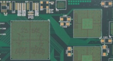
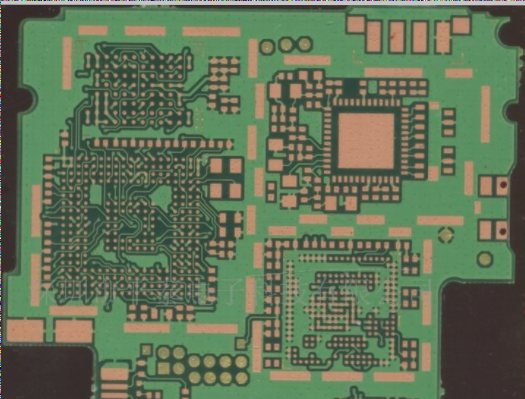
Initial schematic transfer
In the process of transferring the schematic to the layout environment through the netlist file, the device information, netlist, layout information, and initial trace width settings are also transferred.
Here are some recommended steps to prepare for the layout design stage:
1. Set the grid and unit to appropriate values. To achieve more precise control over PCB component and trace layout, set the device grid, copper grid, via grid, and SMD grid to 1 mil.
2. Define the blank area and specify vias for the outer frame of the circuit board according to requirements. PCB manufacturers often specify minimum or recommended values for blind and buried vias.
3. Adjust pad/via parameters based on the capabilities of the PCB manufacturer. Most manufacturers support smaller vias with a 10 mil bore diameter and 20 mil pad diameter.

4. Establish design rules based on requirements.
5. Customize shortcut keys for frequently used layers to enable quick layer switching (and via creation) during routing.
Handling errors in the schematic transfer process:
A common issue in schematic transfer is incorrect or non-existent package assignment. Key considerations include:
If a device in the schematic lacks packaging, a warning message will appear, indicating that the virtual component cannot be exported. Consequently, no default packaging information will transfer to the layout, resulting in the deletion of these components.
If package transfer occurs but the effective package shape doesn’t match correctly, an alarm message will flag this mismatch during transfer.
Correct schematic package assignments or create valid packages for devices. After correction, proceed with forward annotation to update and synchronize design information.
Updating the design with annotations:
Annotation involves transferring design changes between schematic and layout, crucial for maintaining accuracy. Backward labeling (layout to schematic) and forward labeling (schematic to layout) are essential steps.
To safeguard work, always backup and archive current versions of schematic and layout files before significant annotation steps.
Avoid simultaneous changes to schematic and layout. Focus changes on one aspect, then execute appropriate annotation steps to synchronize design data.
Renumbering devices:
Device renumbering organizes PCB components sequentially. Reference numbers should follow a top-to-bottom, left-to-right order on the PCB, aiding assembly, testing, and troubleshooting.
Managing last-minute device or netlist changes:
Although last-minute changes are undesirable, they may be necessary due to component availability or design errors. When altering components or netlists, make changes in the schematic first, then forward annotate to the layout tool.
Additional tips for handling changes:
1. For new devices added post-layout, such as pull-up resistors on open-drain outputs, incorporate resistors and networks in the schematic. Post annotation, these components appear outside the board frame as unplaced items, with connection indicated by flying lines. Position these components on the board frame and perform wiring.
2. Backward labeling and reference label changes can complement each other, like renumbering on the layout rear.
Selecting and positioning devices via highlight:
During PCB layout, utilize the ‘highlight selection’ function to locate specific components or traces in the schematic. This feature is invaluable for matching bypass capacitors with their IC connections. Similarly, it aids in identifying specific components or traces in the layout from the schematic view.


