Principles of RF PCB Board Design
Overview
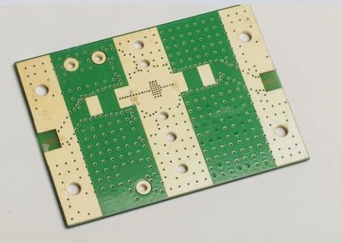
RF PCB board design is a complex process that requires careful consideration of various factors to ensure optimal performance. While it may seem like a “black art” due to theoretical uncertainties, there are specific rules and guidelines that can be followed to achieve success.
Key Considerations
- Impedance and impedance matching
- Materials for insulating layers and laminates
- Wavelength and standing waves
Design Techniques
When designing RF PCB boards, it is essential to isolate high-power RF amplifiers (HPA) and low-noise amplifiers (LNA) to minimize interference. This involves keeping the high-power RF transmitting circuit away from the low-power RF receiving circuit to optimize performance.
Physical and Electrical Zones
Design zones can be classified into physical and electrical zones, each with its own set of considerations. Physical partitioning involves component layout, orientation, and shielding, while electrical partitioning includes sections for power distribution, RF wiring, sensitive circuits and signals, and grounding.
Physical Partitioning
Component layout plays a crucial role in RF design, with the positioning of components along the RF path being particularly important. By minimizing the RF path length and separating high-power and low-power circuits, designers can optimize performance. Additionally, stacking circuit boards with the primary ground layer beneath the surface can help reduce RF energy leakage and improve overall signal integrity.
RF Circuit Isolation
In RF PCB design, it is essential to isolate different RF regions from each other to prevent interference. Techniques such as using linear circuits for multistage amplifiers and implementing diplexers and mixers can help mitigate RF signal interference and ensure optimal performance.
Conclusion
By following these principles and design techniques, PCB designers can create RF boards that meet the demanding requirements of modern mobile phones, ensuring optimal EMC and EMI performance.
Optimizing RF and IF Pathing in PCB Design
When designing a PCB, it is crucial to minimize the crossing of RF and IF paths, keeping them separated as much as possible. The correct RF pathing significantly impacts the overall performance of the PCB, especially in mobile devices. In cell phone PCB designs, a common practice is to place the low-noise amplifier circuit on one side of the board and the high-power amplifier on the opposite side. They are then connected to the RF and baseband processor antenna via a diplexer on the same side.
To prevent RF energy transmission between different sides of the PCB, techniques like using blind holes on both sides can be employed. Straight through-holes should be strategically placed in regions free from RF interference to minimize adverse effects. In cases where isolation between circuit blocks is challenging, a metal shield can be used to contain RF energy within the RF region. However, proper grounding and maintenance of the shield are essential to avoid interference and optimize PCB space.
Decoupling Chip Power for Enhanced Performance
Effective decoupling of chip power is vital, especially for RF chips with integrated linear circuits that are sensitive to power supply noise. Using multiple capacitors and an isolating inductor per chip can help filter out power supply noise. Some chips may require additional power, necessitating multiple sets of capacitors and inductors for proper decoupling.
When decoupling power supplies, it is important to consider the placement of inductors to avoid mutual interference signals. Proper grounding of high-power amplifiers and ensuring RF output remains clear of RF input are critical to prevent signal distortions and oscillations.
Effective Electrical Zoning for Improved Performance
Electrical zoning in PCB design follows similar principles to physical zoning but involves regulating distinct voltages for different phone segments to conserve battery life. Multiple power sources may be required, complicating isolation. Proper grounding and decoupling at the power pin end of high-power amplifiers are essential to prevent noise propagation and ensure stable operation across varying conditions.
Additionally, maintaining proper isolation between RF input and output is crucial to prevent self-excited oscillations and signal distortions. Careful routing of signal lines and filters can significantly impact the performance of the PCB, emphasizing the importance of strategic placement and grounding.
Minimizing Noise in PCB Design
- Anticipated bandwidth span of control line: DC to 2MHz
- VCO control line as part of feedback loop
- Robust RF plane and secure connections
- Adequate decoupling of VCO’s power supply
- Placement of VCO at RF region terminus
- Resonant circuits for transmission and reception
- Sensitivity of resonant circuits to noise
- Close proximity of inductors and capacitors in control loop
Considerations in Mobile Phone PCB Design
When designing PCBs for mobile phones, attention to detail is crucial. Here are some key aspects to consider:
1. Power Supply and Grounding Cables
Proper handling of power and ground cables is essential to prevent noise interference and ensure product quality.
- Importance of decoupling capacitors
- Relationship between ground, power, and signal lines
- Configuration of grounded copper conductors
- Utilization of large copper layer areas for grounding
2. Shared Grounding between Digital and Analog Circuits
Modern PCBs often combine digital and analog circuits, requiring careful consideration to minimize interference, especially in grounding lines.