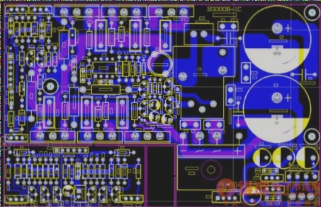
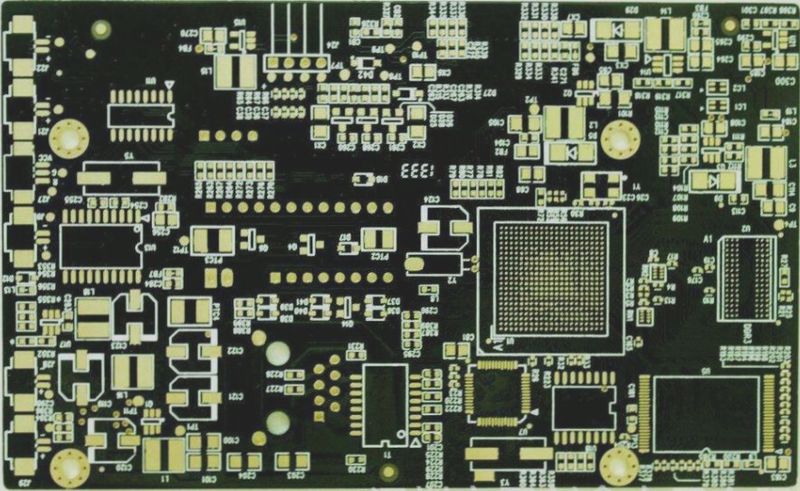
Several issues that should be addressed in the reliability design of PCB boards for high-speed DSP systems.
1. **Power Supply Design**
The foremost consideration in the PCB design of high-speed DSP systems is power supply design. Typically, the following strategies are employed to mitigate signal integrity issues.
2. **Decoupling of Power and Ground**
As DSP operating frequencies increase, DSP and other IC components are often miniaturized and densely packaged. Multi-layer boards are generally utilized in circuit design. It is advisable to allocate a dedicated layer for both power and ground, particularly when dealing with multiple power sources. For instance, the DSP I/O power supply voltage may differ from the core supply voltage, necessitating two separate power supply layers. If multilayer board costs are a concern, a dedicated layer can be allocated for critical power supplies or additional wiring. Power supply routing can follow the same path as signal lines, provided that the line width is adequate.
Regardless of whether the PCB features a dedicated ground or power layer, appropriately distributed capacitors must be placed between the power supply and ground. To conserve space and minimize the number of vias, it is recommended to utilize more chip capacitors. These capacitors can be mounted on the backside of the PCB, that is, the soldering surface, and connected to the vias using wide traces, linking them to both the power supply and ground.

3. Wiring Rules for Power Distribution
Separate Analog and Digital Power Layers
High-speed, high-precision analog components are highly sensitive to digital signals. For instance, amplifiers can amplify switching noise, causing it to resemble pulse signals. Therefore, it is generally required that the power layers for analog and digital sections of the board be kept separate.
Isolate Sensitive Signals
Certain sensitive signals, like high-frequency clocks, are particularly vulnerable to noise interference, necessitating stringent isolation measures. A high-frequency clock (above 20MHz or with a flip time under 5ns) should be accompanied by a dedicated ground wire. The clock trace should be at least 10 mils wide, while the ground escort should be no less than 20 mils. Ensure that holes are well-connected to the ground, with connections every 5cm. Additionally, the clock output should be in series with a damping resistor ranging from 22Ω to 220Ω to mitigate signal noise interference.
Software and Hardware Anti-Jamming Design
Typically, PCB boards for high-speed DSP applications are designed according to specific system requirements. Due to constraints in design capability and lab conditions, inadequate anti-interference measures may lead to electromagnetic interference in less-than-ideal environments, disrupting the DSP program flow. If the DSP cannot revert to its normal operational code, it may crash or even damage components. It’s crucial to implement appropriate anti-jamming strategies.
Hardware Anti-Jamming Design
Hardware anti-jamming is often more effective. When the system’s complexity, cost, and size allow, prioritize hardware solutions. Common hardware anti-jamming techniques can be categorized as follows:
(1) **Hardware Filtering:** RC filters can significantly attenuate various high-frequency interference signals, such as suppressing “burr” interference.
(2) **Reasonable Grounding:** A well-designed grounding system is essential for high-speed digital and analog circuits, providing a low-impedance, large-area ground layer that minimizes EMI and RFI and shields against external interference. Separate the analog ground from the digital ground during PCB design.
(3) **Shielding Measures:** AC power, high-frequency power, and strong current devices can generate electromagnetic waves as noise sources. Metal enclosures can effectively shield these devices and ground them, greatly reducing electromagnetic induction interference.
(4) **Photoelectric Isolation:** Photoelectric isolators can effectively prevent interference between different circuit boards, often used at the DSP interface with devices like sensors and switches.
Software Anti-Jamming Design
Software anti-jamming offers advantages that hardware solutions cannot fully replicate. In DSP applications, it’s essential to maximize the software’s anti-jamming capabilities to reduce interference impacts. Here are several effective software anti-jamming methods:
(1) **Digital Filtering:** Digital filtering can eliminate noise from analog input signals using techniques like median and arithmetic mean filtering.
(2) **Set Trap:** Establish a section of boot code in an unused program area. If the program is disrupted and jumps to this section, the boot code will redirect execution to a designated address and use a special routine to correct errors.
(3) **Instruction Redundancy:** Insert one or two no-operation (NOP) instructions after double-byte or three-byte instructions to help the DSP recover when disrupted.
(4) **Set Watchdog Timer:** To escape “endless loops,” use “watchdog” technology. A timer generates pulses at set intervals, and if the DSP fails to reset the timer, the generated pulse serves as a reset signal, initializing the DSP.
4. Electromagnetic Compatibility Design
Electromagnetic compatibility (EMC) refers to electronic equipment’s ability to function effectively in complex electromagnetic environments. The goal of EMC design is to enable devices to suppress external interference while minimizing their electromagnetic emissions on others. In PCB design, electromagnetic interference, such as crosstalk between adjacent signals, often occurs, influenced by the distributed capacitance and inductance between loops. Several measures can address mutual electromagnetic interference between signals:
5. Choose a Reasonable Wire Width
Transient current impacts on printed traces primarily stem from trace inductance, which is proportional to trace length and inversely proportional to width. Thus, using short, wide traces helps suppress interference. Signal traces for clock leads and bus drivers, which often handle large transient currents, should be minimized in length. For discrete component circuits, a trace width of about 1.5mm is advisable, while for integrated circuits, a width between 0.2mm and 1.0mm is preferred.
Utilize a Tic-Tac-Toe Network Wiring Structure
This method involves routing horizontal traces on the first PCB layer and vertical traces on the subsequent layer.


